101-1101 Rabbit Semiconductor, 101-1101 Datasheet - Page 43
101-1101
Manufacturer Part Number
101-1101
Description
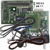
KIT DEV RABBITCORE RCM4110
Manufacturer
Rabbit Semiconductor
Series
RabbitCore 4000r
Type
MPU Moduler
Datasheet
1.20-101-1093.pdf
(112 pages)
Specifications of 101-1101
Contents
RabbitCore Module, Dev. Board, AC Adapter, Cable and Dynamic C® CD-Rom
Processor To Be Evaluated
RCM4110
For Use With/related Products
RCM4110
Lead Free Status / RoHS Status
Lead free by exemption / RoHS compliant by exemption
Other names
316-1076


If a device such as a battery is
connected across two channels
for a differential measurement,
and it is not referenced to
analog ground, then the current
from the device will flow
through both sets of attenuator
resistors without flowing back
to analog ground as shown in
Figure 10. This will generate a
negative voltage at one of the
inputs, LN1, which will almost
certainly lead to inaccurate A/D
conversions. To make such differential measurements, connect the R1 resistors to the A/D
converter’s internal reference voltage, which is software-configurable for 1.15 V, 2.048 V,
or 2.5 V. This internal reference voltage is available on pin 49 of header J3 as VREF, and
allows you to convert analog input voltages that are negative with respect to analog ground.
The A/D converter’s CONVERT pin is available on pin 48 of header J3 and can be used as
a hardware means of forcing the A/D converter to start a conversion cycle at a specific time.
The CONVERT signal is an edge-triggered event and has a hold time of two CCLK periods
for debounce.
A conversion is started by an active (rising) edge on the CONVERT pin. The CONVERT
pin must stay low for at least two CCLK periods before going high for at least two CCLK
periods. Figure 11 shows the timing of a conversion start. The double falling arrow on
CCLK indicates the actual start of the conversion cycle.
Appendix B.4.3 explains the implementation examples of these features on the Prototyp-
ing Board.
User’s Manual
NOTE: The amplifier inside the A/D converter’s internal voltage reference circuit has a
very limited output-current capability. The internal buffer can source up to 20 mA and
sink only up to 200 µA. Use a separate buffer amplifier if you need to supply any load
current.
Figure 11. Timing Diagram for Conversion Start Using CONVERT Pin
Figure 10. Current Flow from Ungrounded
I
or Floating Source
39
Related parts for 101-1101
Image
Part Number
Description
Manufacturer
Datasheet
Request
R

Part Number:
Description:
KIT DEV FOR BL2500 COYOTE
Manufacturer:
Rabbit Semiconductor
Datasheet:

Part Number:
Description:
KIT APPLICATION SIMPLE SENSOR
Manufacturer:
Rabbit Semiconductor
Datasheet:

Part Number:
Description:
KIT DEV RABBITCORE RCM3750
Manufacturer:
Rabbit Semiconductor
Datasheet:

Part Number:
Description:
KIT DEV RABBIT 2000 INT'L
Manufacturer:
Rabbit Semiconductor
Datasheet:
Part Number:
Description:
KIT DEV RABBIT RCM2000 INT'L
Manufacturer:
Rabbit Semiconductor
Datasheet:

Part Number:
Description:
KIT DEVELOPMENT RCM3700 INT'L
Manufacturer:
Rabbit Semiconductor
Datasheet:

Part Number:
Description:
BL4S200 TOOL KIT
Manufacturer:
Rabbit Semiconductor
Datasheet:


Part Number:
Description:
KIT DEVELOPMENT FOR JACKRABBIT
Manufacturer:
Rabbit Semiconductor
Part Number:
Description:
MODULE RABBITCORE RCM3720
Manufacturer:
Rabbit Semiconductor
Datasheet:
Part Number:
Description:
MODULE RABBITCORE RCM3220
Manufacturer:
Rabbit Semiconductor
Datasheet:
Part Number:
Description:
MODULE RABBITCORE RCM3210
Manufacturer:
Rabbit Semiconductor
Datasheet:
Part Number:
Description:
COMPUTER SGL-BOARD OP6600 W/SRAM
Manufacturer:
Rabbit Semiconductor
Datasheet:
Part Number:
Description:
COMPUTER SGL-BD BL2000 SRAM/FLSH
Manufacturer:
Rabbit Semiconductor