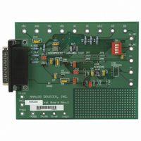
AD5232EVAL10 Analog Devices Inc, AD5232EVAL10 Datasheet - Page 7

AD5232EVAL10
Manufacturer Part Number
AD5232EVAL10
Description
BOARD EVAL 10 FOR AD5232
Manufacturer
Analog Devices Inc
Datasheet
1.AD5232BRUZ100-RL7.pdf
(24 pages)
Specifications of AD5232EVAL10
Rohs Status
RoHS non-compliant
ABSOLUTE MAXIMUM RATINGS
T
Table 3.
Parameter
V
V
V
V
A
Digital Inputs and Output Voltage to GND
Operating Temperature Range
Maximum Junction Temperature (T
Storage Temperature Range
Lead Temperature, Soldering
Package Power Dissipation
1
2
Maximum terminal current is bounded by the maximum current handling of
the switches, maximum power dissipation of the package, and maximum
applied voltage across any two of the A, B, and W terminals at a given
resistance.
Includes programming of nonvolatile memory.
DD
SS
DD
A
A
X
, V
Intermittent
Continuous
Vapor Phase (60 sec)
Infrared (15 sec)
− B
= 25°C, unless otherwise noted.
to GND
to GND
to V
B
, V
X
, A
W
SS
to GND
X
− W
X
1
, B
X
− W
X
2
J
max)
Rating
+0.3 V, −7 V
7 V
±20 mA
±2 mA
−0.3 V, V
−40°C to +85°C
150°C
−65°C to +150°C
220°C
(T
−0.3 V, +7 V
V
215°C
SS
J
− 0.3 V, V
max − T
DD
+ 0.3 V
A
DD
)/θ
+ 0.3 V
JA
Rev. A | Page 7 of 24
Stresses above those listed under Absolute Maximum Ratings
may cause permanent damage to the device. This is a stress
rating only; functional operation of the device at these or any
other conditions above those listed in the operational sections
of this specification is not implied. Exposure to absolute
maximum rating conditions for extended periods may affect
device reliability.
THERMAL RESISTANCE
θ
soldered in a circuit board for surface-mount packages.
Table 4. Thermal Resistance
Package Type
16-Lead TSSOP (RU-16)
ESD CAUTION
JA
is specified for the worst-case conditions, that is, a device
θ
150
JA
θ
28
JC
AD5232
Unit
°C/W


