AD8369-EVAL Analog Devices Inc, AD8369-EVAL Datasheet - Page 16
AD8369-EVAL
Manufacturer Part Number
AD8369-EVAL
Description
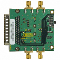
BOARD EVAL FOR AD8369
Manufacturer
Analog Devices Inc
Datasheet
1.AD8369-EVAL.pdf
(24 pages)
Specifications of AD8369-EVAL
Lead Free Status / RoHS Status
Contains lead / RoHS non-compliant


AD8369
For example, suppose the input signal in Figure 4 is a 140 MHz
sinusoid from a ground-referenced 50 W source. The 0.1 mF
coupling capacitors present a very low reactance at this frequency
(11 mW) so that essentially all of the ac voltage is delivered to the
differential inputs of the AD8369. It will be apparent that, in
addition to the use of adequate coupling capacitance, the external
capacitor used to extend the low frequency range of the offset
control loop, C
offset control loop from attempting to track the ac signal fluctuations.
Figure 7. Two-Tone, 70 MHz, 70.3 MHz, –7 dBFS
–100
–100
–10
–20
–30
–40
–50
–60
–70
–80
–90
–10
–20
–30
–40
–50
–60
–70
–80
–90
0
0
Figure 6. Single-Tone 70 MHz, –1 dBFS
0
0
FILT
, must also be large enough to prevent the
5
5
–7dBFS
ADC OUTPUT FREQUENCY – MHz
–72.5dBFS
ADC OUTPUT FREQUENCY – MHz
10
10
INLO
INHI COMM
V
16
S
1
15
15
COMM BIT0
15
2
0.1 F
PWUP VPOS SENB
20
20
14
3
70MHz – 1dBFS
HD2 = –83dBc
HD3 = –80dBc
SNR = 51dB
BIT1
AD8369
13
4
25
25
Figure 5. AD8369 to ADC Interface
BIT2
12
5
0.1 F
30
30
BIT3
FILT CMDC OPHI
11
6
0.1 F
DENB
CONTROL INTERFACE
10
7
–16–
OPLO
8
9
Interfacing to an ADC
The AD8369 can be used to effectively increase the dynamic
range of an ADC in a direct IF sampling receiver application.
Figure 5 provides an example of an interface to an ADC designed
for an IF of 70 MHz. It comprises a low-pass filter that attenuates
harmonics while providing an impedance transformation from
200 W to 1 kW. This impedance transformation allows the AD8369
to operate much below its peak output swing in the pass band,
which significantly reduces distortion.
A high performance 14-bit ADC, the AD6645, is used for illus-
trative purposes and is sampling at 64 MSPs with a full-scale
input of 2.2 V p-p. Typically, an SNR of 51 dB and an SFDR of
almost –90 dBFS are realized by this configuration. Figure 6 shows
an FFT of the AD8369 delivering a single tone at –1 dBFS (that
is, 2 V p-p) at the input of the ADC with an HD2 of –83 dBc and
HD3 of –80 dBc. Figure 7 shows that the two-tone, third-order
intermodulation distortion level is –65.5 dBc.
PCB Layout Considerations
Each input and output pin of the AD8369 presents 100 W
relative to their respective ac grounds. To ensure that signal
integrity is not seriously impaired by the printed circuit board, the
relevant connection traces should provide a characteristic
impedance of 100 W to the ground plane. This can be achieved
through proper layout. Figure 8 shows the cross section of a PC
board and Table II shows the dimensions that will provide a
100 W line impedance.
Table II. Dimensions Required for 100 W Characteristic
Impedance Microstrip Line in FR-4
0.1 F
0.1 F
6.8pF
270nH
270nH
W
H
T
r
(FR-4)
15pF
ADC
4.6
22 mils
53 mils
2.1 mils
1k
REV. 0
Related parts for AD8369-EVAL
Image
Part Number
Description
Manufacturer
Datasheet
Request
R

Part Number:
Description:
BOARD EVAL FOR AD8369 LF-600MHZ
Manufacturer:
Analog Devices Inc

Part Number:
Description:
±1.7g Dual-Axis IMEMS Accelerometer Evaluation Board
Manufacturer:
Analog Devices Inc
Datasheet:
Part Number:
Description:
Inertial Sensor Evaluation System
Manufacturer:
Analog Devices Inc
Datasheet:
Part Number:
Description:
Manufacturer:
Analog Devices Inc
Datasheet:
Part Number:
Description:
Manufacturer:
Analog Devices Inc
Datasheet:
Part Number:
Description:
Manufacturer:
Analog Devices Inc
Datasheet:
Part Number:
Description:
Manufacturer:
Analog Devices Inc
Datasheet:
Part Number:
Description:
Manufacturer:
Analog Devices Inc
Datasheet:
Part Number:
Description:
Manufacturer:
Analog Devices Inc
Datasheet:
Part Number:
Description:
Manufacturer:
Analog Devices Inc
Datasheet:
Part Number:
Description:
Manufacturer:
Analog Devices Inc
Datasheet:
Part Number:
Description:
Manufacturer:
Analog Devices Inc
Datasheet:
Part Number:
Description:
Manufacturer:
Analog Devices Inc
Datasheet: