AD8369-EVAL Analog Devices Inc, AD8369-EVAL Datasheet - Page 19
AD8369-EVAL
Manufacturer Part Number
AD8369-EVAL
Description
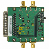
BOARD EVAL FOR AD8369
Manufacturer
Analog Devices Inc
Datasheet
1.AD8369-EVAL.pdf
(24 pages)
Specifications of AD8369-EVAL
Lead Free Status / RoHS Status
Contains lead / RoHS non-compliant


Component
VPOS, GND
SW1
SW2
SW3, R5
SW4
J1, J2, J6, J7
C1, C2, C3, C4
T1, T2
R1, R2, R11, R12
R6, R7, R8, R9, R10 Control Interface Resistors. Simple series resistors for each control interface signal.
C5, C6, C8
C7
C9
REV. 0
Function
Supply and Ground Vector Pins
Data Enable: Set to Position A when in serial mode of operation, set to Position B
when in parallel mode of operation.
Device Enable: When in the PWDN position, the PWUP pin will be connected to
ground and the AD8369 will be disabled. The device is enabled when the switch is
in the PWUP position, connecting the PWUP pin to VPOS.
Serial/Parallel Selection. The device will respond to serial control inputs from
connector P1 when the switch is in the SER position. Parallel operation is achieved
when in the PAR position. Device can be hardwired for parallel mode of operation by
placing the 0 W resistor in position R5.
Parallel Interface Control. Used to hardwire BIT0 through BIT3 to the desired gain
code when in parallel mode of operation. The switch functions as a hexadecimal
to binary encoder (Gain Code 0 = 0000, Gain Code 15 = 1111).
Input and Output Signal Connectors. These SMA connectors provide a convenient
way to interface the evaluation board with 50 W test equipment.
AC-Coupling Capacitors. Provides ac-coupling of the input and output signals.
Impedance Transformers. Used to transform the 200 W input and output
impedance to 50 W.
Single-Ended or Differential. R2 and R11 are used to ground the center tap of
the secondary windings on transformers T1 and T2. R1 and R12 should be used
to ground J2 and J7 when used in single-ended applications. R1 and R12 should be
removed for differential operation.
Power Supply Decoupling. Nominal supply decoupling consists of a 0.1 mF capacitor
to ground followed by a 1 nF capacitor to ground positioned as close to the device
as possible. C8 provides additional decoupling of the input common-mode voltage.
High-Pass Filter Capacitor. Used to set high-pass corner frequency of output.
Clock Filter Capacitor. May be required with some printer ports to minimize overshoot.
The clock waveform may be smoothed using a simple filter network established by
R7 and C9. Some experimentation may be necessary to determine optimum values.
Table III. AD8369 Evaluation Board Configuration Options
–19–
Default Condition
Not Applicable
Not Applicable
Not Applicable
Not Applicable
R5 = Open (Size 0603)
Not Applicable
Not Applicable
C1, C2, C3, C4
= 1 nF (Size 0603)
T1, T2 = TC4-1W
(MiniCircuits)
R1, R2, R11, R12
= 0 W (Size 0603)
R6, R7, R8, R9,
R10 = 0 W (Size 0603)
C5 = 0.1 mF (Size 0603)
C6 = C8 = 1 nF
(Size 0603)
C7 = 0.1 mF (Size 0603)
C9 = Open (Size 0603)
AD8369
Related parts for AD8369-EVAL
Image
Part Number
Description
Manufacturer
Datasheet
Request
R

Part Number:
Description:
BOARD EVAL FOR AD8369 LF-600MHZ
Manufacturer:
Analog Devices Inc

Part Number:
Description:
±1.7g Dual-Axis IMEMS Accelerometer Evaluation Board
Manufacturer:
Analog Devices Inc
Datasheet:
Part Number:
Description:
Inertial Sensor Evaluation System
Manufacturer:
Analog Devices Inc
Datasheet:
Part Number:
Description:
Manufacturer:
Analog Devices Inc
Datasheet:
Part Number:
Description:
Manufacturer:
Analog Devices Inc
Datasheet:
Part Number:
Description:
Manufacturer:
Analog Devices Inc
Datasheet:
Part Number:
Description:
Manufacturer:
Analog Devices Inc
Datasheet:
Part Number:
Description:
Manufacturer:
Analog Devices Inc
Datasheet:
Part Number:
Description:
Manufacturer:
Analog Devices Inc
Datasheet:
Part Number:
Description:
Manufacturer:
Analog Devices Inc
Datasheet:
Part Number:
Description:
Manufacturer:
Analog Devices Inc
Datasheet:
Part Number:
Description:
Manufacturer:
Analog Devices Inc
Datasheet:
Part Number:
Description:
Manufacturer:
Analog Devices Inc
Datasheet: