EVAL-AD1871EB Analog Devices Inc, EVAL-AD1871EB Datasheet - Page 11
EVAL-AD1871EB
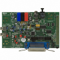
Manufacturer Part Number
EVAL-AD1871EB
Description
BOARD EVAL FOR AD1871
Manufacturer
Analog Devices Inc
Datasheet
1.AD1871YRSZ.pdf
(28 pages)
Specifications of EVAL-AD1871EB
Lead Free Status / RoHS Status
Contains lead / RoHS non-compliant


Pin Function Redefinition in External Control Mode
Pin
No.
2
3
4
5
Pin Function Redefinition in Modulator Mode
Pin
No.
3
25
26
27
28
REV. 0
Input/
Output
I
I
I
I
Input/
Output
O
O
O
O
O
Mnemonic
256/512
DF0
DF1
M/S
Mnemonic
MODCLK
D3
D2
D1
D0
Description
Clock Rate Select. This pin is used to select between an MCLK of 256
512
Data Format Select 0. This pin is used as the low bit (DF0) of the data format selection
(see section on External Control).
Data Format Select 1. This pin is used as the high bit (DF1) of the data format selection
(see section on External Control).
Master/Slave Select. This pin is used to select between the Master (pin low) or Slave (pin
high) Modes.
Description
This pin provides a clock output that allows the user to decode the left and right channel
modulator outputs. It is similar to a left/right clock but runs (nominally) at 5.6448 MHz
and gates a 4-bit modulator output word in each phase (see section on Modulator Mode).
Bit 3 of the Modulator Output Word
Bit 2 of the Modulator Output Word
Bit 1 of the Modulator Output Word
Bit 0 of the Modulator Output Word
f
S
(pin high).
–11–
AD1871
f
S
(pin low) or
Related parts for EVAL-AD1871EB
Image
Part Number
Description
Manufacturer
Datasheet
Request
R

Part Number:
Description:
ENERCHIP CC EVAL KIT
Manufacturer:
Cymbet Corporation
Datasheet:

Part Number:
Description:
BOARD EVAL FOR AD976
Manufacturer:
Analog Devices Inc
Datasheet:

Part Number:
Description:
BOARD EVAL FOR ADXL345
Manufacturer:
Analog Devices Inc
Datasheet:

Part Number:
Description:
ENERCHIP CC SEH EVAL KIT
Manufacturer:
Cymbet Corporation
Datasheet:

Part Number:
Description:
ENERCHIP EP ENERGY HARVEST EVAL
Manufacturer:
Cymbet Corporation
Datasheet:

Part Number:
Description:
EVAL BOARD FOR TW6864-LB2-GR
Manufacturer:
Intersil
Datasheet:
Part Number:
Description:
EVAL BOARD FOR TW8816-LB3-GR
Manufacturer:
Intersil
Datasheet:
Part Number:
Description:
EVAL BOARD FOR TW8817-TA3-GRS
Manufacturer:
Intersil
Datasheet:

Part Number:
Description:
EVALUATION MODULE FOR ADUM4160
Manufacturer:
Analog Devices Inc
Datasheet:

Part Number:
Description:
BOARD EVALUATION ADCMP581BCP
Manufacturer:
Analog Devices Inc
Datasheet:
Part Number:
Description:
BOARD EVALUATION ADM1041
Manufacturer:
Analog Devices Inc
Datasheet:

Part Number:
Description:
EVAL BOARD FOR STM32F107VCT
Manufacturer:
STMicroelectronics
Datasheet:
Part Number:
Description:
BOARD EVAL FOR AD1954
Manufacturer:
Analog Devices Inc
Datasheet:
Part Number:
Description:
BOARD EVAL FOR AD1955
Manufacturer:
Analog Devices Inc
Datasheet:

Part Number:
Description:
BOARD EVAL FOR AD7655
Manufacturer:
Analog Devices Inc
Datasheet: