EVAL-AD5541/42EB Analog Devices Inc, EVAL-AD5541/42EB Datasheet - Page 3
EVAL-AD5541/42EB
Manufacturer Part Number
EVAL-AD5541/42EB
Description
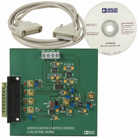
BOARD EVAL FOR AD5541/42
Manufacturer
Analog Devices Inc
Datasheet
1.EVAL-AD554142EB.pdf
(20 pages)
Specifications of EVAL-AD5541/42EB
Number Of Dac's
1
Number Of Bits
16
Outputs And Type
1, Single Ended
Sampling Rate (per Second)
1.5M
Data Interface
Serial
Settling Time
1µs
Dac Type
Voltage
Voltage Supply Source
Single
Operating Temperature
-40°C ~ 85°C
Utilized Ic / Part
AD5541, AD5542
Lead Free Status / RoHS Status
Contains lead / RoHS non-compliant


SPECIFICATIONS
V
Table 1.
Parameter
STATIC PERFORMANCE
OUTPUT CHARACTERISTICS
DAC REFERENCE INPUT
LOGIC INPUTS
REFERENCE
POWER REQUIREMENTS
1
2
3
Temperature ranges are as follows: A, B, C versions: −40°C to +85°C; J, L versions: 0°C to 70°C.
Reference input resistance is code-dependent, minimum at 0x8555.
Guaranteed by design, not subject to production test.
DD
Resolution
Relative Accuracy (INL)
Differential Nonlinearity (DNL)
Gain Error
Gain Error Temperature Coefficient
Zero Code Error
Zero Code Temperature Coefficient
AD5542
Output Voltage Range
Output Voltage Settling Time
Slew Rate
Digital-to-Analog Glitch Impulse
Digital Feedthrough
DAC Output Impedance
Power Supply Rejection Ratio
Reference Input Range
Reference Input Resistance
Input Current
Input Low Voltage, V
Input High Voltage, V
Input Capacitance
Hysteresis Voltage
Reference −3 dB Bandwidth
Reference Feedthrough
Signal-to-Noise Ratio
Reference Input Capacitance
V
I
Power Dissipation
DD
DD
= 5 V ± 10%, V
Bipolar Resistor Matching
Bipolar Zero Offset Error
Bipolar Zero Temperature Coefficient
1
3
3
REF
INL
INH
= 2.5 V, AGND = DGND = 0 V. All specifications T
2
Min
16
0
−V
2.0
9
7.5
2.4
4.50
REF
Typ
±0.5
±0.5
±0.5
±0.5
−1.5
±0.1
0.3
±0.05
1.000
±0.0015
±1
±0.2
1
25
10
10
6.25
0.4
1.3
1
92
75
120
0.3
1.5
Rev. B | Page 3 of 20
Max
±1.0
±2.0
±4.0
±1.0
±1.5
±5
±7
±1
±2
±0.0076
±5
±7
V
V
±1.0
V
±1
0.8
10
5.50
1.1
6.05
REF
REF
DD
− 1 LSB
− 1 LSB
A
= T
MIN
Unit
Bits
LSB
LSB
LSB
LSB
LSB
LSB
LSB
ppm/°C
LSB
LSB
ppm/°C
Ω/Ω
%
LSB
LSB
ppm/°C
V
V
μs
V/μs
nV-sec
nV-sec
kΩ
LSB
V
kΩ
kΩ
μA
V
V
pF
V
MHz
mV p-p
dB
pF
pF
V
mA
mW
to T
MAX
, unless otherwise noted.
Test Conditions
L, C grades
B, J grades
A grade
J grade
T
T
R
T
AD5542 bipolar operation
To 1/2 LSB of FS, C
C
Tolerance typically 20%
ΔV
Unipolar operation
AD5542, bipolar operation
All 1s loaded
Code 0xFFFF
Guaranteed monotonic
Ratio error
Unipolar operation
1 LSB change around the major carry
All 1s loaded to DAC, V
All 0s loaded, V
Code 0x0000
A
A
FB
A
L
= 25° C
= 25° C
= 25° C
= 10 pF, measured from 0% to 63%
/R
DD
INV
± 10%
, typically R
REF
= 1 V p-p at 100 kHz
FB
L
= 10 pF
= R
AD5541/AD5542
REF
INV
= 2.5 V
= 28 kΩ
Related parts for EVAL-AD5541/42EB
Image
Part Number
Description
Manufacturer
Datasheet
Request
R

Part Number:
Description:
IC, ADJ LDO REG, 1.5V TO 5V 250mA MSOP-8
Manufacturer:
Vishay
Datasheet:

Part Number:
Description:
IC, ADJ LDO REG, 1.5V TO 5V 0.6A 8-TSSOP
Manufacturer:
Vishay
Datasheet:
Part Number:
Description:
IC, ADJ LDO REG, 1.5V TO 5V 250mA MSOP-8
Manufacturer:
Vishay
Datasheet:

Part Number:
Description:
IC ADJ LDO REG 1.5V TO 5V 150mA 5-SOT-23
Manufacturer:
Vishay
Datasheet:

Part Number:
Description:
BOARD EVAL AS1324-AD
Manufacturer:
austriamicrosystems
Datasheet:
Part Number:
Description:
IC, ADJ LDO REG, 1.5V TO 5V 0.6A 8-TSSOP
Manufacturer:
Vishay
Datasheet:

Part Number:
Description:
IC, ADJ LDO REG, 1.5V TO 5V, 0.3A, MSOP8
Manufacturer:
Vishay
Datasheet:
Part Number:
Description:
IC, ADJ LDO REG, 1.5V TO 5V, 0.3A, MSOP8
Manufacturer:
Vishay
Datasheet:
Part Number:
Description:
IC, ADJ LDO REG 1.215V TO 5V 0.3A MSOP-8
Manufacturer:
Vishay
Datasheet:
Part Number:
Description:
IC, ADJ LDO REG 1.215V TO 5V 0.3A MSOP-8
Manufacturer:
Vishay
Datasheet:

Part Number:
Description:
±1.7g Dual-Axis IMEMS Accelerometer Evaluation Board
Manufacturer:
Analog Devices Inc
Datasheet:

Part Number:
Description:
IC MULTIPLIER ANALOG 8-SOIC T/R
Manufacturer:
Analog Devices Inc
Datasheet:

Part Number:
Description:
IC ANALOG MULTIPLIER 8-DIP
Manufacturer:
Analog Devices Inc
Datasheet:
Part Number:
Description:
IC ANALOG MULTIPLIER 8-SOIC
Manufacturer:
Analog Devices Inc
Datasheet:
Part Number:
Description:
IC ANALOG MULTIPLIER 8-DIP
Manufacturer:
Analog Devices Inc
Datasheet: