EVAL-AD7671CB Analog Devices Inc, EVAL-AD7671CB Datasheet - Page 18
EVAL-AD7671CB
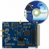
Manufacturer Part Number
EVAL-AD7671CB
Description
BOARD EVAL FOR AD7671
Manufacturer
Analog Devices Inc
Series
PulSAR®r
Datasheet
1.AD7671ASTZ.pdf
(24 pages)
Specifications of EVAL-AD7671CB
Number Of Adc's
1
Number Of Bits
16
Sampling Rate (per Second)
1M
Data Interface
Serial, Parallel
Inputs Per Adc
4 Single Ended
Input Range
±4 REF
Power (typ) @ Conditions
112mW @ 1MSPS
Voltage Supply Source
Analog and Digital
Operating Temperature
-40°C ~ 85°C
Utilized Ic / Part
AD7671
Lead Free Status / RoHS Status
Contains lead / RoHS non-compliant


AD7671
MASTER SERIAL INTERFACE
Internal Clock
The AD7671 is configured to generate and provide the serial data
clock SCLK when the EXT/INT pin is held LOW. It also gener-
ates a SYNC signal to indicate to the host when the serial data is
valid. The serial clock SCLK and the SYNC signal can be inverted
if desired. Depending on RDC/SDIN input, the data can be read
after each conversion or during conversion. Figures 17 and 18
show the detailed timing diagrams of these two modes.
Usually, because the AD7671 is used with a fast throughput, the
mode master, read during conversion, is the most recommended
Serial Mode when it can be used.
SDOUT
Figure 18. Master Serial Data Timing for Reading (Read Previous Conversion during Convert)
CNVST
SDOUT
CS, RD
CS, RD
CNVST
BUSY
SYNC
SCLK
BUSY
SYNC
SCLK
t
16
Figure 17. Master Serial Data Timing for Reading (Read after Convert)
t
3
t
t
t
t
t
14
15
16
14
15
t
t
29
17
X
t
t
22
18
t
EXT/INT = 0
EXT/INT = 0
1
t
3
D15
t
20
X
1
t
22
t
19
t
21
t
20
D14
t
2
D15
23
1
t
t
19
18
RDC/SDIN = 0
RDC/SDIN = 1
D14
t
3
2
t
21
23
–18–
t
28
In Read-during-Conversion Mode, the serial clock and data toggle
at appropriate instants, which minimizes potential feedthrough
between digital activity and the critical conversion decisions.
In Read-after-Conversion Mode, it should be noted that unlike
in other modes, the signal BUSY returns LOW after the 16 data
bits are pulsed out and not at the end of the conversion phase,
which results in a longer BUSY width.
While the AD7671 is performing a bit decision, it is important that
voltage transients not occur on digital input/output pins or degra-
dation of the conversion result could occur. This is particularly
important during the second half of the conversion phase because
3
14
D2
INVSCLK = INVSYNC = 0
INVSCLK = INVSYNC = 0
14
D2
15
D1
15
D1
16
t
24
t
16
30
D0
t
24
D0
t
t
t
t
t
t
25
25
27
26
26
27
REV. B
Related parts for EVAL-AD7671CB
Image
Part Number
Description
Manufacturer
Datasheet
Request
R

Part Number:
Description:
ENERCHIP CC EVAL KIT
Manufacturer:
Cymbet Corporation
Datasheet:

Part Number:
Description:
BOARD EVAL FOR AD976
Manufacturer:
Analog Devices Inc
Datasheet:

Part Number:
Description:
BOARD EVAL FOR ADXL345
Manufacturer:
Analog Devices Inc
Datasheet:

Part Number:
Description:
ENERCHIP CC SEH EVAL KIT
Manufacturer:
Cymbet Corporation
Datasheet:

Part Number:
Description:
ENERCHIP EP ENERGY HARVEST EVAL
Manufacturer:
Cymbet Corporation
Datasheet:

Part Number:
Description:
EVAL BOARD FOR TW6864-LB2-GR
Manufacturer:
Intersil
Datasheet:
Part Number:
Description:
EVAL BOARD FOR TW8816-LB3-GR
Manufacturer:
Intersil
Datasheet:
Part Number:
Description:
EVAL BOARD FOR TW8817-TA3-GRS
Manufacturer:
Intersil
Datasheet:

Part Number:
Description:
EVALUATION MODULE FOR ADUM4160
Manufacturer:
Analog Devices Inc
Datasheet:

Part Number:
Description:
BOARD EVALUATION ADCMP581BCP
Manufacturer:
Analog Devices Inc
Datasheet:
Part Number:
Description:
BOARD EVALUATION ADM1041
Manufacturer:
Analog Devices Inc
Datasheet:

Part Number:
Description:
EVAL BOARD FOR STM32F107VCT
Manufacturer:
STMicroelectronics
Datasheet:
Part Number:
Description:
BOARD EVAL FOR AD1954
Manufacturer:
Analog Devices Inc
Datasheet:
Part Number:
Description:
BOARD EVAL FOR AD1955
Manufacturer:
Analog Devices Inc
Datasheet:

Part Number:
Description:
BOARD EVAL FOR AD7655
Manufacturer:
Analog Devices Inc
Datasheet: