EVAL-AD7731EB Analog Devices Inc, EVAL-AD7731EB Datasheet - Page 4
EVAL-AD7731EB
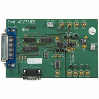
Manufacturer Part Number
EVAL-AD7731EB
Description
BOARD EVAL FOR AD7731
Manufacturer
Analog Devices Inc
Specifications of EVAL-AD7731EB
Number Of Adc's
1
Number Of Bits
24
Sampling Rate (per Second)
6.4k
Data Interface
Serial
Inputs Per Adc
3 Differential
Input Range
±1.28 V
Power (typ) @ Conditions
67.5mW @ 6.4kSPS
Voltage Supply Source
Analog and Digital
Operating Temperature
-40°C ~ 85°C
Utilized Ic / Part
AD7731
Lead Free Status / RoHS Status
Contains lead / RoHS non-compliant


EVAL-AD7731EB
Table III. SKT2 Pin Designations
1
2
3
4
5
6
7-8
9
10
11-12
13
14-18
19-30
31-36
N C
D I N
SCLK
N C
DV
N C
D O U T
N C
D G N D
N C
DD
36
18
No Connect. This pin is not connected on the evaluation board.
Serial Data Input. Data applied to this pin is buffered before being applied to the AD7731's DIN pin. The
serial data applied to the DIN pin is written to the input shift register on the part. Data from this input
shift register is transferred to one of the on-chip registers depending on the register selection bits of the
Communications Register.
Reset Input. The signal on this pin is buffered before being applied to the
digital filter and all on-chip registers to power-on status.
Chip Select. The signal on this pin is buffered before being applied to the
an active low logic input used to select the AD7731. With this input hard-wired low, the AD7731 operates
in its three-wire interface mode with SCLK, DIN and DOUT used to interface to the device.
used to select the device in systems with more than one device on the serial bus or as a frame synchronisation
signal in communicating with the AD7731.
Serial Clock. The signal on this pin is buffered before being applied to the SCLK pin of the AD7731.
An external serial clock is applied to this input to access serial data from the AD7731. This serial clock
can be a continuous clock with all data transmitted in a continuous train of pulses. Alternatively, it can
be a non-continuous clock with the information being transmitted to the AD7731 in smaller batches of
data.
Logic Input. The signal on this pin is buffered before being applied to the
AD7731s. While
control logic are reset and the analog modulator is also held in its reset state.
No Connect. These pins are not connected on the evaluation board.
Digital Supply Voltage. This provides the supply voltage for IC4, the buffer chip which buffers the output
signals from the AD7731 before they are applied to SKT2.
Logic output. This is a buffered version of the signal on the AD7731's
output in both conversion and calibration mode. In conversion mode, a logic low on the
indicates that a new output word is available from the AD7731 data register. The
upon completion of a read operation of a full output word. If no data read has taken place after an output
update, the
taking place and return low again. This gives an indication of when a read operation should not be initiated
to avoid reading from the data register as it is being updated. In calibration mode,
calibration is initiated and returns low to indicate that calibration is complete.
No Connect. These pins are not connected on the evaluation board.
Serial Data Output. This is a buffered version of the signal on the AD7731's DOUT pin. Serial data from
the output shift register on the part is clocked out on this pin. This output shift register contains
information from one of the nine on-chip registers depending on the register selection bits of the
Communications Register.
No Connect. These pins are not connected on the evaluation board.
Ground reference point for digital circuitry. Connects to the DGND plane on the evaluation board.
No Connect. These pins are not connected on the evaluation board.
input allows for synchronisation of the digital filters and analog modulators across a number of
is an active low input which resets the control logic, interface logic, calibration coefficients,
line will return high prior to the next output update, remain high while the update is
is low, the nodes of the digital filter, the filter control logic, and the calibration
Figure 3. SKT2 Pin Configuration
–4–
pin.
pin of the AD7731.
pin of the AD7731. The
pin of the AD7731.
pin will return high
is used as a status
goes high when
19
1
REV. A
can be
output
is
Related parts for EVAL-AD7731EB
Image
Part Number
Description
Manufacturer
Datasheet
Request
R

Part Number:
Description:
ENERCHIP CC EVAL KIT
Manufacturer:
Cymbet Corporation
Datasheet:

Part Number:
Description:
BOARD EVAL FOR AD976
Manufacturer:
Analog Devices Inc
Datasheet:

Part Number:
Description:
BOARD EVAL FOR ADXL345
Manufacturer:
Analog Devices Inc
Datasheet:

Part Number:
Description:
ENERCHIP CC SEH EVAL KIT
Manufacturer:
Cymbet Corporation
Datasheet:

Part Number:
Description:
ENERCHIP EP ENERGY HARVEST EVAL
Manufacturer:
Cymbet Corporation
Datasheet:

Part Number:
Description:
EVAL BOARD FOR TW6864-LB2-GR
Manufacturer:
Intersil
Datasheet:
Part Number:
Description:
EVAL BOARD FOR TW8816-LB3-GR
Manufacturer:
Intersil
Datasheet:
Part Number:
Description:
EVAL BOARD FOR TW8817-TA3-GRS
Manufacturer:
Intersil
Datasheet:

Part Number:
Description:
EVALUATION MODULE FOR ADUM4160
Manufacturer:
Analog Devices Inc
Datasheet:

Part Number:
Description:
BOARD EVALUATION ADCMP581BCP
Manufacturer:
Analog Devices Inc
Datasheet:
Part Number:
Description:
BOARD EVALUATION ADM1041
Manufacturer:
Analog Devices Inc
Datasheet:

Part Number:
Description:
EVAL BOARD FOR STM32F107VCT
Manufacturer:
STMicroelectronics
Datasheet:
Part Number:
Description:
BOARD EVAL FOR AD1954
Manufacturer:
Analog Devices Inc
Datasheet:
Part Number:
Description:
BOARD EVAL FOR AD1955
Manufacturer:
Analog Devices Inc
Datasheet:

Part Number:
Description:
BOARD EVAL FOR AD7655
Manufacturer:
Analog Devices Inc
Datasheet: