EVAL-AD9831EB Analog Devices Inc, EVAL-AD9831EB Datasheet - Page 6
EVAL-AD9831EB
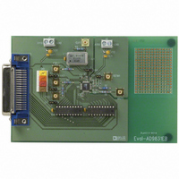
Manufacturer Part Number
EVAL-AD9831EB
Description
BOARD EVAL FOR AD9831
Manufacturer
Analog Devices Inc
Type
Direct Digital Synthesis (DDS)r
Datasheet
1.EVAL-AD9831EB.pdf
(16 pages)
Specifications of EVAL-AD9831EB
Contents
Evaluation Board
For Use With/related Products
AD9831
Lead Free Status / RoHS Status
Contains lead / RoHS non-compliant


AD9831
TERMINOLOGY
Integral Nonlinearity
This is the maximum deviation of any code from a straight line
passing through the endpoints of the transfer function. The
endpoints of the transfer function are zero scale, a point 0.5
LSB below the first code transition (000 . . . 00 to 000 . . . 01)
and full scale, a point 0.5 LSB above the last code transition
(111 . . . 10 to 111 . . . 11). The error is expressed in LSBs.
Differential Nonlinearity
This is the difference between the measured and ideal 1 LSB
change between two adjacent codes in the DAC.
Signal to (Noise + Distortion)
Signal to (Noise + Distortion) is measured signal to noise at the
output of the DAC. The signal is the rms magnitude of the
fundamental. Noise is the rms sum of all the nonfundamental
signals up to half the sampling frequency (f
ing the dc component. Signal to (Noise + Distortion) is
dependent on the number of quantization levels used in the
digitization process; the more levels, the smaller the quantiza-
tion noise. The theoretical Signal to (Noise + Distortion) ratio
for a sine wave input is given by
where N is the number of bits. Thus, for an ideal 10-bit con-
verter, Signal to (Noise + Distortion) = 61.96 dB.
Total Harmonic Distortion
Total Harmonic Distortion (THD) is the ratio of the rms sum
of harmonics to the rms value of the fundamental. For the
AD9831, THD is defined as
where V
V
sixth harmonic.
Output Compliance
The output compliance refers to the maximum voltage which
can be generated at the output of the DAC to meet the specifi-
cations. When voltages greater than that specified for the
output compliance are generated, the AD9831 may not meet
the specifications listed in the data sheet.
Spurious Free Dynamic Range
Along with the frequency of interest, harmonics of the funda-
mental frequency and images of the MCLK frequency are
present at the output of a DDS device. The spurious free dy-
namic range (SFDR) refers to the largest spur or harmonic
which is present in the band of interest. The wide band SFDR
gives the magnitude of the largest harmonic or spur relative to
the magnitude of the fundamental frequency in the bandwidth
4
, V
MSB
D15
D15
X
5
and V
Signal to (Noise + Distortion) = (6.02N + 1.76) dB
1
is the rms amplitude of the fundamental and V
THD 20 log
D14
X
6
are the rms amplitudes of the second through the
D13
X
(V
D12
2
X
2
V
3
2
MSB
D11
V
V
1
4
2
MCLK
V
5
2
Table III. Frequency Register Bits
/2) but exclud-
V
Table IV. Phase Register Bits
6
2
2
, V
3
,
–6–
SFDR gives the attenuation of the largest spur or harmonic in a
bandwidth of
Clock Feedthrough
There will be feedthrough from the MCLK input to the analog
output. Clock feedthrough refers to the magnitude of the
MCLK signal relative to the fundamental frequency in the
AD9831’s output spectrum.
A2
0
0
0
0
1
1
1
1
Register
FREQ0 REG
FREQ1 REG
PHASE0 REG 12 Bits
PHASE1 REG 12 Bits
PHASE2 REG 12 Bits
PHASE3 REG 12 Bits
2 MHz about the fundamental frequency. The narrow band
Table II. Addressing the Control Registers
A1
0
0
1
1
0
0
1
1
50 kHz about the fundamental frequency.
Size
32 Bits
32 Bits
Table I. Control Registers
A0
0
1
0
1
0
1
0
1
Description
Frequency Register 0. This de-
fines the output frequency, when
FSELECT = 0, as a fraction of the
MCLK frequency.
Frequency Register 1. This de-
fines the output frequency, when
FSELECT = 1, as a fraction of the
MCLK frequency.
Phase Offset Register 0. When
PSEL0 = PSEL1 = 0, the contents
of this register are added to the
output of the phase accumulator.
Phase Offset Register 1. When
PSEL0 = 1 and PSEL1 = 0, the con-
tents of this register are added to
the output of the phase accumulator.
Phase Offset Register 2. When
PSEL0 = 0 and PSEL1 = 1, the con-
tents of this register are added to
the output of the phase accumulator.
Phase Offset Register 3. When
PSEL0 = PSEL1 = 1, the contents
of this register are added to the
output of the phase accumulator.
Destination Register
FREQ0 REG 16 LSBs
FREQ0 REG 16 MSBs
FREQ1 REG 16 LSBs
FREQ1 REG 16 MSBs
PHASE0 REG
PHASE1 REG
PHASE2 REG
PHASE3 REG
D0
LSB
D0
LSB
REV. A
Related parts for EVAL-AD9831EB
Image
Part Number
Description
Manufacturer
Datasheet
Request
R

Part Number:
Description:
ENERCHIP CC EVAL KIT
Manufacturer:
Cymbet Corporation
Datasheet:

Part Number:
Description:
BOARD EVAL FOR AD976
Manufacturer:
Analog Devices Inc
Datasheet:

Part Number:
Description:
BOARD EVAL FOR ADXL345
Manufacturer:
Analog Devices Inc
Datasheet:

Part Number:
Description:
ENERCHIP CC SEH EVAL KIT
Manufacturer:
Cymbet Corporation
Datasheet:

Part Number:
Description:
ENERCHIP EP ENERGY HARVEST EVAL
Manufacturer:
Cymbet Corporation
Datasheet:

Part Number:
Description:
EVAL BOARD FOR TW6864-LB2-GR
Manufacturer:
Intersil
Datasheet:
Part Number:
Description:
EVAL BOARD FOR TW8816-LB3-GR
Manufacturer:
Intersil
Datasheet:
Part Number:
Description:
EVAL BOARD FOR TW8817-TA3-GRS
Manufacturer:
Intersil
Datasheet:

Part Number:
Description:
EVALUATION MODULE FOR ADUM4160
Manufacturer:
Analog Devices Inc
Datasheet:

Part Number:
Description:
BOARD EVALUATION ADCMP581BCP
Manufacturer:
Analog Devices Inc
Datasheet:
Part Number:
Description:
BOARD EVALUATION ADM1041
Manufacturer:
Analog Devices Inc
Datasheet:

Part Number:
Description:
EVAL BOARD FOR STM32F107VCT
Manufacturer:
STMicroelectronics
Datasheet:
Part Number:
Description:
BOARD EVAL FOR AD1954
Manufacturer:
Analog Devices Inc
Datasheet:
Part Number:
Description:
BOARD EVAL FOR AD1955
Manufacturer:
Analog Devices Inc
Datasheet:

Part Number:
Description:
BOARD EVAL FOR AD7655
Manufacturer:
Analog Devices Inc
Datasheet: