SSM2167-EVAL Analog Devices Inc, SSM2167-EVAL Datasheet - Page 9
SSM2167-EVAL
Manufacturer Part Number
SSM2167-EVAL
Description
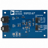
BOARD EVAL FOR SSM2167
Manufacturer
Analog Devices Inc
Datasheet
1.SSM2167-1RMZ-REEL.pdf
(12 pages)
Specifications of SSM2167-EVAL
Rohs Status
RoHS non-compliant


LEVEL DETECTOR
The SSM2167 incorporates a full-wave rectifier and a true rms
level detector circuit whose averaging time constant is set by an
external capacitor (C
For optimal low frequency operation of the level detector down
to 10 Hz, the value of the capacitor should be 2.2 μF. Some experi-
mentation with larger values for C
the effects of excessive low frequency ambient background noise.
The value of the averaging capacitor affects sound quality: too
small a value for this capacitor may cause a pumping effect for
some signals, whereas too large a value can result in slow response
times to signal dynamics. Electrolytic capacitors are recommended
here for lowest cost and should be in the range of 2 μF to 22 μF.
The rms detector filter time constant is approximately given by
10 × C
controls both the steady state averaging in the rms detector as well
as the release time for compression, that is, the time it takes for
the system gain to increase due to a decrease in input signal. The
attack time, the time it takes for the gain to be reduced because
of a sudden increase in input level, is controlled mainly by internal
circuitry that speeds up the attack for large level changes. In most
cases, this limits overload time to less than 35 ms.
The performance of the rms level detector is illustrated in
Figure 14 for a C
In Figure 13 and Figure 14, the input signal to the SSM2167
(not shown) is a series of tone bursts in six successive 10 dB
steps. The tone bursts range from −66 dBV (0.5 mV rms) to
−6 dBV (0.5 V rms). As illustrated in these figures, the attack
time of the rms level detector is dependent only on C
release times are linear ramps whose decay times are dependent
on both C
approximately 240 dB/s for a C
C
CONTROL CIRCUITRY
The output of the rms level detector is a signal proportional to
the log of the true rms value of the buffer output with an added
dc offset. The control circuitry subtracts a dc voltage from this
signal, scales it, and sends the result to the VCA to control the
gain. The gain control of the VCA is logarithmic—a linear change
in control signal causes a dB change in gain. It is this control
law that allows linear processing of the log rms signal to provide
the flat compression characteristic on the input/output charac-
teristic shown in Figure 2.
AVG
of 22 μF.
AVG
milliseconds where C
AVG
and the input signal step size. The rate of release is
AVG
of 2.2 μF and Figure 13 for a C
AVG
) connected to the AVG CAP (Pin 6).
AVG
AVG
AVG
of 2.2 μF, and 12 dB/s for a
is in μF. This time constant
may be necessary to reduce
AVG
AVG
of 22 μF.
, but the
Rev. F | Page 9 of 12
SETTING THE COMPRESSION RATIO
Changing the scaling of the control signal fed to the VCA causes
a change in the circuit compression ratio, r. This effect is shown
in Figure 17. Connecting a resistor (R
V
compression ratios as indicated in Table 4. AGC performance is
achieved with compression ratios between 2:1 and 10:1, and is
dependent on the application. Shorting R
function, setting the compression equal to 1:1. If using a compres-
sion resistor, using a value greater than 5 kΩ is recommended.
If a value lower than 5 kΩ is used, the device may interpret this
as a short, 0 Ω.
Table 4. Setting Compression Ratio
Compression Ratio
1:1
2:1
3:1
5:1
10:1
DD
sets the compression ratio. Lowering R
Figure 17. Effect of Varying the Compression Ratio
V
DE
10:1
5:1
2:1
1:1
1
INPUT (dB)
1
Value of R
0 Ω (short to V+)
15 kΩ
35 kΩ
75 kΩ
175 kΩ
COMP
V
RP
COMP
) between Pin 8 and
COMP
COMP
disables the AGC
VCA GAIN
gives smaller
SSM2167
Related parts for SSM2167-EVAL
Image
Part Number
Description
Manufacturer
Datasheet
Request
R

Part Number:
Description:
IC PREAMP AUDIO MONO AB 10MSOP
Manufacturer:
Analog Devices Inc
Datasheet:
Part Number:
Description:
IC PREAMP AUDIO MONO AB 10MSOP
Manufacturer:
Analog Devices Inc
Datasheet:
Part Number:
Description:
IC PREAMP AUDIO MONO AB 10MSOP
Manufacturer:
Analog Devices Inc
Datasheet:
Part Number:
Description:
IC PREAMP AUDIO MONO AB 10MSOP
Manufacturer:
Analog Devices Inc
Datasheet:
Part Number:
Description:
MICROPHONE PREAMP W/18dB FIXED GAIN
Manufacturer:
Analog Devices Inc
Datasheet:

Part Number:
Description:
±1.7g Dual-Axis IMEMS Accelerometer Evaluation Board
Manufacturer:
Analog Devices Inc
Datasheet:

Part Number:
Description:
Inertial Sensor Evaluation System
Manufacturer:
Analog Devices Inc
Datasheet:
Part Number:
Description:
Manufacturer:
Analog Devices Inc
Datasheet:
Part Number:
Description:
Manufacturer:
Analog Devices Inc
Datasheet:
Part Number:
Description:
Manufacturer:
Analog Devices Inc
Datasheet:
Part Number:
Description:
Manufacturer:
Analog Devices Inc
Datasheet:
Part Number:
Description:
Manufacturer:
Analog Devices Inc
Datasheet:
Part Number:
Description:
Manufacturer:
Analog Devices Inc
Datasheet: