AD8221-EVAL Analog Devices Inc, AD8221-EVAL Datasheet - Page 17
AD8221-EVAL
Manufacturer Part Number
AD8221-EVAL
Description
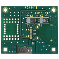
BOARD EVAL FOR AD8221
Manufacturer
Analog Devices Inc
Datasheet
1.AD8221-EVAL.pdf
(24 pages)
Specifications of AD8221-EVAL
Design Resources
Low Cost, High Voltage, Programmable Gain Instrumentation Amplifier Using AD5292 and AD8221 (CN0114) Low Cost Programmable Gain Instrumentation Amplifier Circuit Using ADG1611 and AD620 (CN0146)
Module/board Type
Evaluation Board
For Use With/related Products
AD8221
Lead Free Status / RoHS Status
Contains lead / RoHS non-compliant
Other names
Q1815689


THEORY OF OPERATION
The AD8221 is a monolithic instrumentation amplifier based
on the classic 3-op amp topology. Input transistors Q1 and Q2
are biased at a fixed current so that any differential input signal
forces the output voltages of A1 and A2 to change accordingly.
A signal applied to the input creates a current through R
and R2, such that the outputs of A1 and A2 deliver the correct
voltage. Topologically, Q1, A1, R1 and Q2, A2, R2 can be
viewed as precision current feedback amplifiers. The amplified
differential and common-mode signals are applied to a
difference amplifier that rejects the common-mode voltage
but amplifies the differential voltage. The difference amplifier
employs innovations that result in low output offset voltage as
well as low output offset voltage drift. Laser-trimmed resistors
allow for a highly accurate in-amp with gain error typically less
than 20 ppm and CMRR that exceeds 90 dB (G = 1).
Using superbeta input transistors and an I
scheme, the AD8221 offers extremely high input impedance,
low I
extremely low voltage noise of 8 nV/√Hz.
The transfer function of the AD8221 is
Users can easily and accurately set the gain using a single
standard resistor.
B
G
, low I
=
1+
B
49
I
B
–IN
drift, low I
COMPENSATION
4 .
R
G
kΩ
+V
S
400Ω
OS
–V
, low input bias current noise, and
S
Q1
I
C1
R1 24.7kΩ
B
A1
compensation
+V
–V
S
S
R
G
V
Figure 43. Simplified Schematic
B
G
, R1,
+V
–V
R2
Rev. C | Page 17 of 24
S
S
A2
24.7kΩ
C2
Q2
Because the input amplifiers employ a current feedback
architecture, the gain-bandwidth product of the AD8221
increases with gain, resulting in a system that does not suffer
from the expected bandwidth loss of voltage feedback
architectures at higher gains.
To maintain precision even at low input levels, special attention
was given to the design and layout of the AD8221, resulting in
an in-amp whose performance satisfies the most demanding
applications.
A unique pinout enables the AD8221 to meet a CMRR
specification of 80 dB at 10 kHz (G = 1) and 110 dB at 1 kHz
(G = 1000). The balanced pinout, shown in Figure 44, reduces
the parasitics that had, in the past, adversely affected CMRR
performance. In addition, the new pinout simplifies board
layout because associated traces are grouped together. For
example, the gain setting resistor pins are adjacent to the
inputs, and the reference pin is next to the output.
I
–V
I
B
COMPENSATION
S
400Ω
+V
S
10kΩ
10kΩ
+IN
+IN
–IN
R
R
G
G
Figure 44. Pinout Diagram
1
2
3
4
10kΩ
TOP VIEW
AD8221
A3
10kΩ
+V
–V
S
S
8
7
6
5
+V
V
REF
–V
OUT
+V
–V
S
S
S
S
OUTPUT
REF
AD8221
Related parts for AD8221-EVAL
Image
Part Number
Description
Manufacturer
Datasheet
Request
R

Part Number:
Description:
AD8221/6/8/9 SO Pkg Eval Bd
Manufacturer:
Analog Devices Inc
Datasheet:

Part Number:
Description:
±1.7g Dual-Axis IMEMS Accelerometer Evaluation Board
Manufacturer:
Analog Devices Inc
Datasheet:
Part Number:
Description:
Inertial Sensor Evaluation System
Manufacturer:
Analog Devices Inc
Datasheet:
Part Number:
Description:
Manufacturer:
Analog Devices Inc
Datasheet:
Part Number:
Description:
Manufacturer:
Analog Devices Inc
Datasheet:
Part Number:
Description:
Manufacturer:
Analog Devices Inc
Datasheet:
Part Number:
Description:
Manufacturer:
Analog Devices Inc
Datasheet:
Part Number:
Description:
Manufacturer:
Analog Devices Inc
Datasheet:
Part Number:
Description:
Manufacturer:
Analog Devices Inc
Datasheet:
Part Number:
Description:
Manufacturer:
Analog Devices Inc
Datasheet:
Part Number:
Description:
Manufacturer:
Analog Devices Inc
Datasheet:
Part Number:
Description:
Manufacturer:
Analog Devices Inc
Datasheet:
Part Number:
Description:
Manufacturer:
Analog Devices Inc
Datasheet: