AD8221-EVAL Analog Devices Inc, AD8221-EVAL Datasheet - Page 21
AD8221-EVAL
Manufacturer Part Number
AD8221-EVAL
Description
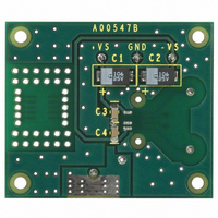
BOARD EVAL FOR AD8221
Manufacturer
Analog Devices Inc
Datasheet
1.AD8221-EVAL.pdf
(24 pages)
Specifications of AD8221-EVAL
Design Resources
Low Cost, High Voltage, Programmable Gain Instrumentation Amplifier Using AD5292 and AD8221 (CN0114) Low Cost Programmable Gain Instrumentation Amplifier Circuit Using ADG1611 and AD620 (CN0146)
Module/board Type
Evaluation Board
For Use With/related Products
AD8221
Lead Free Status / RoHS Status
Contains lead / RoHS non-compliant
Other names
Q1815689


In this topology, an
AD8221. The output signal of the instrumentation amplifier is
taken across the OUT pin and the REF pin. Two 1 kΩ resistors
and a 499 Ω resistor attenuate the ±10 V signal to +4 V. An
optional capacitor, C1, can serve as an antialiasing filter. An
AD8022 is used to drive the ADC.
This topology has five benefits. In addition to level-shifting and
attenuation, very little noise is contributed to the system. Noise
from R1 and R2 is common to both of the inputs of the ADC
and is easily rejected. R5 adds a third of the dominant noise and
therefore makes a negligible contribution to the noise of the
system. The attenuator divides the noise from R3 and R4. Likewise,
its noise contribution is negligible. The fourth benefit of this
interface circuit is that the acquisition time of the AD8221 is
reduced by a factor of 2. With the help of the OP27, the AD8221
only needs to deliver one-half of the full swing; therefore, signals
can settle more quickly. Lastly, the AD8022 settles quickly,
which is helpful because the shorter the settling time, the
more bits that can be resolved when the ADC acquires data.
This configuration provides attenuation, a level-shift, and a
convenient interface with a differential input ADC while
maintaining performance.
AC-COUPLED INSTRUMENTATION AMPLIFIER
Measuring small signals that are in the noise or offset of the
amplifier can be a challenge. Figure 52 shows a circuit that can
improve the resolution of small ac signals. The large gain
OP27
sets the reference voltage of the
Rev. C | Page 21 of 24
reduces the referred input noise of the amplifier to 8 nV/√Hz.
Thus, smaller signals can be measured because the noise floor is
lower. DC offsets that would have been gained by 100 are
eliminated from the output of the AD8221 by the integrator
feedback network.
At low frequencies, the
0 V. Once a signal exceeds f
amplified input signal.
499Ω
0.1µF
0.1µF
R
+IN
–IN
10µF
AD8221
+V
+V
–V
S
S
S
Figure 52. AC-Coupled Circuit
10µF
OP1177
–V
REF
S
HIGH-PASS
forces the output of the AD8221 to
0.1µF
0.1µF
f
1µF
HIGH-PASS
, the AD8221 outputs the
C
+V
–V
OP1177
=
S
S
2πRC
1
15.8kΩ
AD8221
R
Related parts for AD8221-EVAL
Image
Part Number
Description
Manufacturer
Datasheet
Request
R

Part Number:
Description:
AD8221/6/8/9 SO Pkg Eval Bd
Manufacturer:
Analog Devices Inc
Datasheet:

Part Number:
Description:
±1.7g Dual-Axis IMEMS Accelerometer Evaluation Board
Manufacturer:
Analog Devices Inc
Datasheet:
Part Number:
Description:
Inertial Sensor Evaluation System
Manufacturer:
Analog Devices Inc
Datasheet:
Part Number:
Description:
Manufacturer:
Analog Devices Inc
Datasheet:
Part Number:
Description:
Manufacturer:
Analog Devices Inc
Datasheet:
Part Number:
Description:
Manufacturer:
Analog Devices Inc
Datasheet:
Part Number:
Description:
Manufacturer:
Analog Devices Inc
Datasheet:
Part Number:
Description:
Manufacturer:
Analog Devices Inc
Datasheet:
Part Number:
Description:
Manufacturer:
Analog Devices Inc
Datasheet:
Part Number:
Description:
Manufacturer:
Analog Devices Inc
Datasheet:
Part Number:
Description:
Manufacturer:
Analog Devices Inc
Datasheet:
Part Number:
Description:
Manufacturer:
Analog Devices Inc
Datasheet:
Part Number:
Description:
Manufacturer:
Analog Devices Inc
Datasheet: