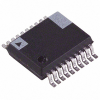
ADE7761ARS-REF Analog Devices Inc, ADE7761ARS-REF Datasheet - Page 15

ADE7761ARS-REF
Manufacturer Part Number
ADE7761ARS-REF
Description
IC ENERGY METERING 20-SSOP
Manufacturer
Analog Devices Inc
Datasheet
1.ADE7761ARS-REF.pdf
(28 pages)
Specifications of ADE7761ARS-REF
Rohs Status
RoHS non-compliant
output (and, therefore, the bit stream) approaches that of the
input signal level. For any given input value in a single sampling
interval, the data from the 1-bit ADC is virtually meaningless.
Only when a large number of samples are averaged is a
meaningful result obtained. This averaging is carried out in the
second part of the ADC, the digital low-pass filter. By averaging
a large number of bits from the modulator, the low-pass filter
can produce 24-bit data words that are proportional to the input
signal level.
The Σ-Δ converter uses two techniques to achieve high
resolution from what is essentially a 1-bit conversion technique.
The first is oversampling, which means that the signal is
sampled at a rate (frequency) that is many times higher than the
bandwidth of interest. For example, the sampling rate in the
ADE7761 is CLKIN (450 kHz) and the band of interest is 40 Hz
to 1 kHz. Oversampling has the effect of spreading the
quantization noise (noise due to sampling) over a wider
bandwidth. With the noise spread more thinly over a wider
bandwidth, the quantization noise in the band of interest is
lowered (see Figure 18).
However, oversampling alone is not an efficient enough method
to improve the signal-to-noise ratio (SNR) in the band of inter-
est. For example, an oversampling ratio of 4 is required just to
increase the SNR by only 6 dB (1 bit). To keep the oversampling
ratio at a reasonable level, it is possible to shape the quantization
noise so that the majority of the noise lies at the higher frequen-
cies. This is what happens in the Σ-Δ modulator; the noise is
shaped by the integrator, which has a high-pass type response
for the quantization noise. The result is that most of the noise is
at the higher frequencies where it can be removed by the digital
low-pass filter. This noise shaping is also shown in Figure 18.
SIGNAL
SIGNAL
NOISE
NOISE
0
0
Figure 18. Noise Reduction Due to Oversampling and
1kHz
1kHz
HIGH RESOLUTION
OUTPUT FROM
DIGITAL FILTER
Noise Shaping in the Analog Modulator
DIGITAL LFP
ANTIALIAS FILTER (RC)
FREQUENCY (Hz)
FREQUENCY (Hz)
225kHz
225kHz
SHAPED NOISE
SAMPLING FREQUENCY
450kHz
450kHz
Rev. A | Page 15 of 28
Antialias Filter
Figure 18 also shows an analog low-pass filter (RC) on input to
the modulator. This filter is present to prevent aliasing. Aliasing
is an artifact of all sampled systems, which means that fre-
quency components in the input signal to the ADC that are
higher than half the sampling rate of the ADC appear in the
sampled signal frequency below half the sampling rate.
Figure 19 illustrates the effect.
In Figure 19, frequency components (arrows shown in black)
above half the sampling frequency (also known as the Nyquist
frequency), that is, 225 kHz, are imaged or folded back down
below 225 kHz (arrows shown in gray). This happens with all
ADCs no matter what the architecture. In the example shown,
only frequencies near the sampling frequency (450 kHz) move
into the band of interest for metering (40 Hz to 1 kHz). This
fact allows the use of a very simple low-pass filter to attenuate
these frequencies (near 250 kHz) and thereby prevent distortion
in the band of interest. A simple RC filter (single pole) with a
corner frequency of 10 kHz produces an attenuation of
approximately 33 dB at 450 kHz (see Figure 19). This is
sufficient to eliminate the effects of aliasing.
ACTIVE POWER CALCULATION
The ADCs digitize the voltage signals from the current and
voltage transducers. A high-pass filter in the current channel
removes any dc component from the current signal. This
eliminates any inaccuracies in the active power calculation due
to offsets in the voltage or current signals (see the HPF and
Offset Effects section).
The active power calculation is derived from the instantaneous
power signal. The instantaneous power signal is generated by a
direct multiplication of the current and voltage signals. To
extract the active power component (dc component), the
instantaneous power signal is low-pass filtered. Figure 20
illustrates the instantaneous active power signal and shows how
the active power information can be extracted by low-pass
filtering the instantaneous power signal. This scheme correctly
calculates active power for nonsinusoidal current and voltage
waveforms at all power factors. All signal processing is carried
out in the digital domain for superior stability over temperature
and time.
Figure 19. ADC and Signal Processing in Current Channel or Voltage Channel
0
1kHz
FREQUENCIES
IMAGE
ANTIALIASING EFFECTS
FREQUENCY (Hz)
225kHz
450kHz
FREQUENCY
SAMPLING
ADE7761


