EVAL-AD5390EB Analog Devices Inc, EVAL-AD5390EB Datasheet - Page 33
EVAL-AD5390EB
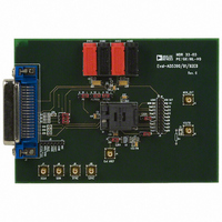
Manufacturer Part Number
EVAL-AD5390EB
Description
BOARD EVAL FOR AD5390
Manufacturer
Analog Devices Inc
Specifications of EVAL-AD5390EB
Number Of Dac's
16
Number Of Bits
14
Outputs And Type
16, Single Ended
Sampling Rate (per Second)
125k
Data Interface
Serial
Settling Time
8µs
Dac Type
Voltage
Voltage Supply Source
Single
Operating Temperature
-40°C ~ 85°C
Utilized Ic / Part
AD5390
Lead Free Status / RoHS Status
Contains lead / RoHS non-compliant


Table 27 shows the control register contents of the AD5391. Table 28 provides bit descriptions. Note that REG1 = REG0 = 0,
A3 to A0 = 1100, and DB13 to DB0 contain the control register data.
Table 27. AD5391 Control Register Contents
MSB
CR11
Table 28. AD5391 Bit Descriptions
Bit
CR11
CR10
CR9
CR8
CR7
CR6
CR5 to CR2
CR1 to CR0
CR10
Description
Power-Down Status. This bit is used to configure the output amplifier state in power-down mode.
CR11 = 1: Amplifier output is high impedance (default on power-up).
CR11 = 0: Amplifier output is 100 kΩ to ground.
REF Select. This bit selects the operating internal reference for the AD5391. CR10 is programmed as follows:
CR10 = 1: Internal reference is 2.5 V (AD5391-5 default). Recommended operating reference for AD5391-5.
CR10 = 0: Internal reference is 1.25 V (AD5391-3 default). Recommended operating reference for AD5391-3.
Current Boost Control. This bit is used to boost the current in the output amplifier, thus altering its slew rate. This bit is
configured as follows:
CR9 = 1: Boost mode on. This maximizes the bias current in the output amplifier, optimizing its slew rate but increasing
the power dissipation.
CR9 = 0: Boost mode off (default on power-up). This reduces the bias current in the output amplifier and reduces the overall
power consumption.
Internal/External Reference. This bits determines if the DAC uses its internal reference or an external reference.
CR8 = 1: Internal reference enabled. Reference output depends on data loaded to CR10.
CR8 = 0: External reference selected (default on power-up).
Channel Monitor Enable (see Table 24).
CR7 = 1: Monitor enabled. This enables the channel monitor function. Following a write to the monitor channel in
the SFR register, the selected channel output is routed to the MON_OUT pin.
CR7 = 0: Monitor disabled (default on power-up). When monitor is disabled, the MON_OUT pin is three-stated.
Thermal Monitor Function. When enabled, this function is used to monitor the internal die temperature of the AD5391,
when enabled. The thermal monitor powers down the output amplifiers when the temperature exceeds 130°C. This function
can be used to protect the device in cases where the power dissipation of the device may be exceeded, if a number of
output channels are simultaneously short circuited. A soft power-up re-enables the output amplifiers if the die temperature
has dropped below 130°C.
CR6 = 1: Thermal monitor enabled.
CR6 = 0: Thermal monitor disabled (default on power-up).
Don’t Care.
Toggle Function Enable. This function lets the user toggle the output between two codes loaded to the A and B register for
each DAC. Control Register Bit CR1 and Bit CR0 are used to enable individual groups of eight channels for operation in
toggle mode on the AD5391, as follows:
CR1
CR0
Logic 1 written to any bit enables a group of channels and Logic 0 disables a group. LDAC is used to toggle between the two
registers.
Group 1
Group 0
CR9
Channel 8 to Channel 15
Channel 0 to Channel 7
CR8
CR7
Rev. C | Page 33 of 40
CR6
CR5
CR4
CR3
AD5390/AD5391/AD5392
CR2
CR1
LSB
CR0
Related parts for EVAL-AD5390EB
Image
Part Number
Description
Manufacturer
Datasheet
Request
R

Part Number:
Description:
ENERCHIP CC EVAL KIT
Manufacturer:
Cymbet Corporation
Datasheet:

Part Number:
Description:
BOARD EVAL FOR AD976
Manufacturer:
Analog Devices Inc
Datasheet:

Part Number:
Description:
BOARD EVAL FOR ADXL345
Manufacturer:
Analog Devices Inc
Datasheet:

Part Number:
Description:
ENERCHIP CC SEH EVAL KIT
Manufacturer:
Cymbet Corporation
Datasheet:

Part Number:
Description:
ENERCHIP EP ENERGY HARVEST EVAL
Manufacturer:
Cymbet Corporation
Datasheet:

Part Number:
Description:
EVAL BOARD FOR TW6864-LB2-GR
Manufacturer:
Intersil
Datasheet:
Part Number:
Description:
EVAL BOARD FOR TW8816-LB3-GR
Manufacturer:
Intersil
Datasheet:
Part Number:
Description:
EVAL BOARD FOR TW8817-TA3-GRS
Manufacturer:
Intersil
Datasheet:

Part Number:
Description:
EVALUATION MODULE FOR ADUM4160
Manufacturer:
Analog Devices Inc
Datasheet:

Part Number:
Description:
BOARD EVALUATION ADCMP581BCP
Manufacturer:
Analog Devices Inc
Datasheet:
Part Number:
Description:
BOARD EVALUATION ADM1041
Manufacturer:
Analog Devices Inc
Datasheet:

Part Number:
Description:
EVAL BOARD FOR STM32F107VCT
Manufacturer:
STMicroelectronics
Datasheet:
Part Number:
Description:
BOARD EVAL FOR AD1954
Manufacturer:
Analog Devices Inc
Datasheet:
Part Number:
Description:
BOARD EVAL FOR AD1955
Manufacturer:
Analog Devices Inc
Datasheet:

Part Number:
Description:
BOARD EVAL FOR AD7655
Manufacturer:
Analog Devices Inc
Datasheet: