EVAL-AD5381EB Analog Devices Inc, EVAL-AD5381EB Datasheet - Page 6
EVAL-AD5381EB
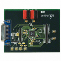
Manufacturer Part Number
EVAL-AD5381EB
Description
BOARD EVAL FOR AD5381
Manufacturer
Analog Devices Inc
Specifications of EVAL-AD5381EB
Rohs Status
RoHS non-compliant
Number Of Dac's
40
Number Of Bits
12
Outputs And Type
40, Single Ended
Sampling Rate (per Second)
167k
Data Interface
DSP, I²C, MICROWIRE™, Parallel, QSPI™, SPI™
Settling Time
6µs
Dac Type
Voltage
Voltage Supply Source
Single
Operating Temperature
-40°C ~ 85°C
Utilized Ic / Part
AD5381


AD5381
AD5381-3 SPECIFICATIONS
AVDD = 2.7 V to 3.6 V; DVDD = 2.7 V to 5.5 V, AGND = DGND = 0 V; external REFIN = 1.25 V;
all specifications T
Table 4.
Parameter
ACCURACY
REFERENCE INPUT/OUTPUT
OUTPUT CHARACTERISTICS
MONITOR PIN
LOGIC INPUTS (EXCEPT SDA/SCL)
LOGIC INPUTS (SDA, SCL ONLY)
Resolution
Relative Accuracy
Differential Nonlinearity (DNL)
Zero-Scale Error
Offset Error
Offset Error TC
Gain Error
Gain Temperature Coefficient
DC Crosstalk
Reference Input
Reference Input Voltage
DC Input Impedance
Input Current
Reference Range
Reference Output
Output Voltage
Reference TC
Output Voltage Range
Short-Circuit Current
Load Current
Capacitive Load Stability
DC Output Impedance
Output Impedance
Three-State Leakage Current
V
V
Input Current
Pin Capacitance
V
V
I
V
C
Glitch Rejection
IN
IH
IL,
IH
IL
HYST
IN
, Input Leakage Current
R
R
, Input Low Voltage
, Input High Voltage
, Input High Voltage
, Input Capacitance
Input Low Voltage
L
L
, Input Hysteresis
= ∞
= 5 kΩ
3
3
MIN
2
4
(INL)
to T
2
MAX
3
, unless otherwise noted.
3
3
AD5381-3
12
±1
±1
4
±4
±5
±0.024
±0.1
2
0.5
1.25
±10
1 to AVDD/2
1.245/1.255
2.47/2.53
±10
±15
0/AVDD
40
±1
200
1000
0.5
500
100
2
0.8
±10
10
0.7 DVDD
0.3 DVDD
±1
0.05 DVDD
8
50
1
1
LSB max
LSB max
LSB max
V
V min/max
V min/max
ppm/°C max
V min/max
mA max
pF max
μA max
pF max
V max
Unit
Bits
mV max
mV max
μV/°C typ
% FSR max
% FSR max
ppm FSR/°C typ
MΩ min
μA max
V min/max
ppm/°C max
mA max
pF max
Ω max
Ω typ
nA typ
V min
V max
V min
μA max
V min
pF typ
ns max
Rev. B | Page 6 of 40
Test Conditions/Comments
Output unloaded
Guaranteed monotonic over temperature
Measured at Code 64 in the linear region
At 25 °C
T
±1% for specified performance
Typically 100 MΩ
Typically ±30 nA
Enabled via CR8 in the AD5381 control register
CR10 selects the reference voltage.
At ambient; optimized for 1.25 V operation; CR10 = 0
CR10 = 1
Temperature Range: +25°C to +85°C
Temperature Range: –40°C to +85°C
DVDD = 2.7 V to 3.6 V
Total for all pins; T
SMBus compatible at DVDD < 3.6 V
SMBus compatible at DVDD < 3.6 V
Input filtering suppresses noise spikes of less than 50 ns
MIN
to T
MAX
A
= T
MIN
to T
MAX
Related parts for EVAL-AD5381EB
Image
Part Number
Description
Manufacturer
Datasheet
Request
R

Part Number:
Description:
ENERCHIP CC EVAL KIT
Manufacturer:
Cymbet Corporation
Datasheet:

Part Number:
Description:
BOARD EVAL FOR AD976
Manufacturer:
Analog Devices Inc
Datasheet:

Part Number:
Description:
BOARD EVAL FOR ADXL345
Manufacturer:
Analog Devices Inc
Datasheet:

Part Number:
Description:
ENERCHIP CC SEH EVAL KIT
Manufacturer:
Cymbet Corporation
Datasheet:

Part Number:
Description:
ENERCHIP EP ENERGY HARVEST EVAL
Manufacturer:
Cymbet Corporation
Datasheet:

Part Number:
Description:
EVAL BOARD FOR TW6864-LB2-GR
Manufacturer:
Intersil
Datasheet:
Part Number:
Description:
EVAL BOARD FOR TW8816-LB3-GR
Manufacturer:
Intersil
Datasheet:
Part Number:
Description:
EVAL BOARD FOR TW8817-TA3-GRS
Manufacturer:
Intersil
Datasheet:

Part Number:
Description:
EVALUATION MODULE FOR ADUM4160
Manufacturer:
Analog Devices Inc
Datasheet:

Part Number:
Description:
BOARD EVALUATION ADCMP581BCP
Manufacturer:
Analog Devices Inc
Datasheet:
Part Number:
Description:
BOARD EVALUATION ADM1041
Manufacturer:
Analog Devices Inc
Datasheet:

Part Number:
Description:
EVAL BOARD FOR STM32F107VCT
Manufacturer:
STMicroelectronics
Datasheet:
Part Number:
Description:
BOARD EVAL FOR AD1954
Manufacturer:
Analog Devices Inc
Datasheet:
Part Number:
Description:
BOARD EVAL FOR AD1955
Manufacturer:
Analog Devices Inc
Datasheet:

Part Number:
Description:
BOARD EVAL FOR AD7655
Manufacturer:
Analog Devices Inc
Datasheet: