STEVAL-ISA021V1 STMicroelectronics, STEVAL-ISA021V1 Datasheet - Page 4
STEVAL-ISA021V1
Manufacturer Part Number
STEVAL-ISA021V1
Description
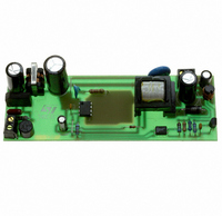
BOARD REF VIPER22A SGL OUTPUT
Manufacturer
STMicroelectronics
Series
VIPER™r
Datasheet
1.STEVAL-ISA035V1.pdf
(17 pages)
Specifications of STEVAL-ISA021V1
Design Resources
STEVAL-ISA021V1 Gerber Files STEVAL-ISA021V1 Schematic STEVAL-ISA021V1 Bill of Material
Main Purpose
AC/DC, Primary Side
Outputs And Type
1, Isolated
Power - Output
10W
Voltage - Output
12V
Current - Output
840mA
Voltage - Input
90 ~ 264VAC
Regulator Topology
Flyback
Frequency - Switching
60kHz
Board Type
Fully Populated
Utilized Ic / Part
VIPer22A
Product
Power Management Modules
Lead Free Status / RoHS Status
Lead free by exemption / RoHS compliant by exemption
Other names
497-5219
Available stocks
Company
Part Number
Manufacturer
Quantity
Price


Circuit operation
1
1.1
1.2
4/17
Circuit operation
Input line rectification and line conducted filter
The circuit operations for all four versions are basically the same. The difference is in the
circuit for startup. Version 1 will be described here with reference to
the converter is not isolated from the input. This makes neutral common to output ground
thus giving a reference back to neutral. The buck is less expensive due to the fact that it
does not use a transformer and an opto coupler. The AC line is applied through D1 which
rectifies the line input every other half cycle.
C1, L0, C2 form a pie filter to reduce EMI noise. The value of the capacitor is chosen to
maintain a reasonable valley, because the caps are charged every other half cycle. Two
diodes can be used in place of D1 to sustain burst pulses of 2 kV. R10 serves two purposes,
one is for inrush limiting and the other is to act as a fuse in case of a catastrophic failure. A
wire wound resistor handles the energy of the inrush. Flame proof resistor and a fuse can be
used depending on system and safety requirements. C7 helps the EMI by balancing line and
neutral noise without using an Xcap. This will pass EN55022 level "B". If the requirement is
less, then this cap can be left out of the circuit.
Start circuit
The voltage across C2 is fed to the drain, pin 5 through 8. Inside the VIPer, the constant
current source delivers 1mA to the V
the V
pulsing. During this time, the energy is being supplied from the V
must be greater than the energy needed to supply the output current plus the energy to
charge of the output capacitor, before the V
Figure 8
startup time. During a short circuit, the V
the internal high voltage current generator to initiate a new startup sequence. The charging
and discharging of the capacitor determine the time period that the power supply is to be on
and off. This reduces the RMS heating effect on all components. The regulation circuit
consists of Dz, C4 and D8. D8 peak charges C4 during the freewheeling time when D5 is
conducting. During this time, the source or reference to the VIPer is one diode drop below
ground, which compensates for the D8 drop. So basically the Zener voltage is the same as
the output voltage. C4 is connected across V
is a BZT52C12, ½ W Zener with a specified test current of 5 mA. These Zeners that are
specified at a lower current give better accuracy of the output voltage. If the output voltage is
lower than 16 V, the circuit can be configured as in
V
case condition. A 16 V Zener with a 5% low tolerance can be 15.2 V plus the internal
resistance to ground is 1230 Ω which is an additional 1.23 V for a total of 16.4 V. For 16 V
output and higher, the V
similar to
fb
pin. When the internal current source charges the V
dd
pin reaches 14.5 V nominal, the current source turns off and the VIPer starts
and
Figure
Figure
4.
9. The value of the capacitor is therefore chosen to accommodate the
dd
pin and the V
dd
pin 4. This current charges C3. When the voltage on
fb
dd
pin can share a common diode and capacitor filter
cap discharges below the minim value enabling
dd
fb
cap falls below 9 V. This can be seen in
and source to filter the regulation voltage. Dz
Figure 3
dd
cap, V
where V
dd
dd
can reach 16V at worse
cap. The energy stored
dd
Figure
is separated from the
3. The output of
AN2544
Related parts for STEVAL-ISA021V1
Image
Part Number
Description
Manufacturer
Datasheet
Request
R

Part Number:
Description:
BOARD RGB CTR ST7,STP08C596MTR
Manufacturer:
STMicroelectronics
Datasheet:

Part Number:
Description:
Power Management IC Development Tools Full Speed USB to RS232 Bridge Demo
Manufacturer:
STMicroelectronics
Datasheet:
Part Number:
Description:
Power Management IC Development Tools 2.5W solar eval BRD USB SPV1040 LD39050
Manufacturer:
STMicroelectronics
Datasheet:

Part Number:
Description:
BOARD EVAL FOR MEMS SENSORS
Manufacturer:
STMicroelectronics
Datasheet:

Part Number:
Description:
KIT DEV STARTER ST10F276Z5
Manufacturer:
STMicroelectronics
Datasheet:

Part Number:
Description:
BOARD EVAL HDMI $ VIDEO SWITCH
Manufacturer:
STMicroelectronics
Datasheet:

Part Number:
Description:
BOARD DEMO ACCELEROMETER DIL24
Manufacturer:
STMicroelectronics
Datasheet:

Part Number:
Description:
BOARD STLM75/STDS75/ST72F651
Manufacturer:
STMicroelectronics
Datasheet:

Part Number:
Description:
EVAL BOARD 3AXIS MEMS ACCELLRMTR
Manufacturer:
STMicroelectronics
Datasheet:

Part Number:
Description:
BOARD EVAL 8BIT MICRO + TDE1708
Manufacturer:
STMicroelectronics
Datasheet:
Part Number:
Description:
STMicroelectronics [RIPPLE-CARRY BINARY COUNTER/DIVIDERS]
Manufacturer:
STMicroelectronics
Datasheet:
Part Number:
Description:
STMicroelectronics [LIQUID-CRYSTAL DISPLAY DRIVERS]
Manufacturer:
STMicroelectronics
Datasheet:
Part Number:
Description:
BOARD EVAL FOR MEMS SENSORS
Manufacturer:
STMicroelectronics
Datasheet: