DK-NIOS-2C35N Altera, DK-NIOS-2C35N Datasheet - Page 51
DK-NIOS-2C35N
Manufacturer Part Number
DK-NIOS-2C35N
Description
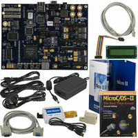
NIOS II KIT W/CYCLONE II EP2C35N
Manufacturer
Altera
Series
Cyclone® IIr
Type
Nios®IIr
Specifications of DK-NIOS-2C35N
Contents
Eval Board, Design Apps, Software, Cables and Accessories
For Use With/related Products
Cyclone ll 2C35N
Lead Free Status / RoHS Status
Lead free / RoHS Compliant
Other names
544-1698
DK-NIOS-2C35N
DK-NIOS-2C35N
Available stocks
Company
Part Number
Manufacturer
Quantity
Price


JTAG Connectors
(J24 & J5)
Altera Corporation
May 2007
User Configuration
The user configuration partition is 1 MB, starting at offset 0x00C00000.
This section contains the FPGA configuration data for the user
configuration. Nios II development tools include documentation on how
to create your own user configuration image and program it into flash
memory.
Factory Configuration
The factory configuration partition is 1 MB, starting at offset 0x00E00000.
This section contains the FPGA configuration data for the factory
configuration. The Nios II processor system in the factory configuration
is designed to start executing code from offset 0x00000000 in the flash
memory. The Nios II development tools include the source files for the
factory programmed hardware and software reference designs.
Persistent Data
The persistent data partition is 64 KB, starting at offset 0x00FF0000. This
partition is for maintaining nonvolatile settings and data, such as the
MAC address and IP address for the factory-programmed web server
reference design. Persistent data is technically no different than other
application data, but it is often convenient to think of certain data as
independent from the user hardware or software.
The Nios development board has two 10-pin JTAG headers (J24 and J5)
compatible with Altera download cables, such as the USB-Blaster™. On
the Nios development board, each JTAG header connects to one Altera
device and forms a single-device JTAG chain. J24 connects to the FPGA
(U62), and J5 connects to the EPM7256AE device (U3).
JTAG Connector to FPGA (J24)
J24 connects to the JTAG pins (TCK, TDI, TDO, TMS, TRST) of the FPGA
(U62) as shown in
configure the FPGA with a new hardware image via an Altera download
cable as shown in
Nios II processor JTAG debug module via a download cable connected to
the J24 JTAG connector.
Reference Manual
Figure
Figure
2–19. In addition, the Nios II IDE can access the
2–18. Altera Quartus II software can directly
Nios Development Board Cyclone II Edition
Board Components
2–39
Related parts for DK-NIOS-2C35N
Image
Part Number
Description
Manufacturer
Datasheet
Request
R

Part Number:
Description:
NIOS II KIT W/STRATIX II EP2S60N
Manufacturer:
Altera
Datasheet:

Part Number:
Description:
CYCLONE II STARTER KIT EP2C20N
Manufacturer:
Altera
Datasheet:

Part Number:
Description:
KIT DEV NIOS II CYCLONE III ED.
Manufacturer:
Altera
Datasheet:

Part Number:
Description:
KIT DEV MAXII W/EPM 1270N
Manufacturer:
Altera
Datasheet:

Part Number:
Description:
DK-SLSR30-300N EZS RCVR NI HSG 30mm X 300mm NO PKG
Manufacturer:
BANNER ENGINEERING


Part Number:
Description:
CPLD, EP610 Family, ECMOS Process, 300 Gates, 16 Macro Cells, 16 Reg., 16 User I/Os, 5V Supply, 35 Speed Grade, 24DIP
Manufacturer:
Altera Corporation
Datasheet:
Part Number:
Description:
CPLD, EP610 Family, ECMOS Process, 300 Gates, 16 Macro Cells, 16 Reg., 16 User I/Os, 5V Supply, 15 Speed Grade, 24DIP
Manufacturer:
Altera Corporation
Datasheet:
Part Number:
Description:
Manufacturer:
Altera Corporation
Datasheet:
Part Number:
Description:
CPLD, EP610 Family, ECMOS Process, 300 Gates, 16 Macro Cells, 16 Reg., 16 User I/Os, 5V Supply, 30 Speed Grade, 24DIP
Manufacturer:
Altera Corporation
Datasheet:
Part Number:
Description:
High-performance, low-power erasable programmable logic devices with 8 macrocells, 10ns
Manufacturer:
Altera Corporation
Datasheet:
Part Number:
Description:
High-performance, low-power erasable programmable logic devices with 8 macrocells, 7ns
Manufacturer:
Altera Corporation
Datasheet:
Part Number:
Description:
Classic EPLD
Manufacturer:
Altera Corporation
Datasheet:
Part Number:
Description:
High-performance, low-power erasable programmable logic devices with 8 macrocells, 10ns
Manufacturer:
Altera Corporation
Datasheet: