DK-NIOS-2S60N Altera, DK-NIOS-2S60N Datasheet
DK-NIOS-2S60N
Specifications of DK-NIOS-2S60N
Available stocks


Related parts for DK-NIOS-2S60N


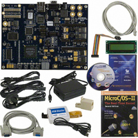
DK-NIOS-2S60N Summary of contents
Page 1
... Reference Manual, Stratix II Edition 101 Innovation Drive San Jose, CA 95134 (408) 544-7000 http://www.altera.com Nios Development Board Preliminary Information ...
Page 2
... Altera Corporation in the U.S. and other countries. All other product or service names are the property of their respective holders. Al- tera products are protected under numerous U ...
Page 3
... About this Manual .................................................................................. v How to Find Information ......................................................................................................................... v How to Contact Altera ............................................................................................................................ vi Typographic Conventions ..................................................................................................................... vii Introduction ......................................................................................... 1 Features Overview ................................................................................................................................. 1–1 General Description ............................................................................................................................... 1–1 Board Components ................................................................................. 5 Component List ...................................................................................................................................... 2–5 Stratix II Device (U60) ........................................................................................................................... 2–7 Push-Button Switches (SW0 - SW3) .................................................................................................... 2–9 Individual LEDs (D0 - D7) .................................................................................................................... 2–9 Seven-Segment LEDs (U8 & U9) ....................................................................................................... 2–10 SRAM Memory (U35 & ...
Page 4
... Reprogramming the EPM7128AE Configuration Controller Device ............................................ B–1 Connecting to the Board via Ethernet 1 Introduction ........................................................................................................................................... C–1 Connecting the Ethernet Cable ........................................................................................................... C–1 Connecting the LCD Screen ................................................................................................................ C–2 Obtaining an IP Address ..................................................................................................................... C–2 LAN Connection .............................................................................................................................. C–3 DHCP ........................................................................................................................................... C–3 Static IP Address ........................................................................................................................ C–3 Point–to–Point Connections .......................................................................................................... C–4 Browsing to Your Board ...................................................................................................................... C–5 iv Altera Corporation ...
Page 5
... July 2005 October 2004 September 2004 ■ How to Find Information ■ ■ ■ Altera Corporation July 2005 About this Manual II Edition. ™ Date Updated for the EP2S30 device. Updated the heat sink illustrations. First publication of Nios Development Board Reference Manual, Stratix II Edition The Adobe Acrobat Find feature allows you to search the contents of a PDF file ...
Page 6
... Altera literature services lit_req@altera.com (1) Non-technical customer (800) 767-3753 service FTP site ftp.altera.com Note to table: (1) You can also contact your local Altera sales office or sales representative. vi USA & Canada altera.com/mysupport/ (408) 544-7000 (7:00 a.m. to 5:00 p.m. Pacific Time) www.altera.com lit_req@altera.com (1) (408) 544-7000 (7:30 a ...
Page 7
... The warning indicates information that should be read prior to starting or w continuing the procedure or processes r The angled arrow indicates you should press the Enter key. f The feet direct you to more information on a particular topic. Altera Corporation July 2005 Meaning , \qdesigns directory, d: drive, chiptrip.gdf file. MAX , PIA ...
Page 8
... Typographic Conventions viii Altera Corporation July 2005 ...
Page 9
... Features The Nios development board, Stratix II Edition, provides a hardware platform for developing embedded systems based on Altera Stratix II Overview devices. The Nios development board, Stratix II Edition provides the following features: ■ ■ ■ ■ ■ ■ ■ ■ ■ ■ ■ ■ ...
Page 10
... M-RAM blocks. The issue can be worked around easily, but some consideration is required when migrating designs based on this device to a non-ES device. There is a label near the FPGA; if the letters “ES” appear on the label, the device is an engineering sample. Altera Corporation July 2005 ...
Page 11
... For further information on the default reference design, see Appendix C, Connecting to the Board via In the course of development, you may overwrite or erase the flash memory space containing the default reference design. Altera provides the flash image for the default reference design so you can return the board to its default state. See ...
Page 12
... Factory-Programmed Reference Design 1–4 Nios Development Board Reference Manual, Stratix II Edition Altera Corporation July 2005 ...
Page 13
... GERBER files for the development board are installed in the Nios II development kit documents directory. See descriptions of all features of the board. Figure 2–1. Nios Development Board Altera Corporation July 2005 Board Components Figure 2–1). A complete set of schematics, a Figure 2–1 and Table 2– ...
Page 14
... Mictor connector for debugging Nios II systems using a First Silicon Solutions (FS2) debug probe. Connects to the FPGA allowing hardware configuration from Quartus II software and software debug from the Nios II IDE. Connects to the configuration controller Altera EPM7128AE device used to configure the FPGA from flash memory Description Altera Corporation July 2005 ...
Page 15
... Adaptive look-up tables (ALUTs) Equivalent LEs M512 RAM blocks M4K RAM blocks M-RAM blocks Total RAM bits DSP blocks Altera Corporation July 2005 Name in the FPGA Push-button switch to reconfigure the FPGA with the factory- programmed reference design Push-button switch to reset the board ...
Page 16
... For Stratix II-related documentation including Stratix II pinout data refer to the Altera Stratix II literature page at www.altera.com/ literature/lit- stx2.html. Early shipments of the board had a heat sink mounted on the Stratix II FPGA. Boards shipped later than May 2005 do not include the heat sink, because thermal management is unnecessary for the majority of FPGA designs for this board ...
Page 17
... Stratix II device. See (D0 - D7) purpose I/O pins on the Stratix II device as shown in Stratix II pin drives logic 1, the corresponding LED turns on. Table 2–4. LED Pin Out Table Altera Corporation July 2005 Table 2–3. Each Stratix II device pin will see a logic 0 Stratix II Pin ...
Page 18
... The SRAM devices share address and data connections with the flash memory and the Ethernet MAC/PHY device. For shared bus information, see 2–10 Nios Development Board Reference Manual, Stratix II Edition Appendix A, Shared Bus Table. Figure 2–3 for Altera Corporation July 2005 ...
Page 19
... For details see section Partitions” on page f See www.amd.com for detailed information about the flash memory device. Altera Corporation July 2005 A Nios II embedded processor implemented on the Stratix II device can use the flash as general-purpose readable memory and non- volatile storage. ...
Page 20
... DQ4 8 DQ5 10 DQ6 11 DQ7 13 DQ8 74 DQ9 76 DQ10 77 DQ11 79 DQ12 80 Connects to Stratix II Pin AD4 AD3 AD5 W9 W10 AB10 AF5 AE5 AC6 AF6 AA10 Y9 AE23 AD23 W15 V14 AA16 AD16 AF17 AD17 AF18 AA17 V16 AB17 AF19 AD18 AD19 Altera Corporation July 2005 ...
Page 21
... Table 2–5. SDRAM (U57) Pin Table (Part Refer to www.micron.com for detailed information. Altera Corporation July 2005 Pin Name Pin Number DQ13 82 DQ14 83 DQ15 85 DQ16 31 DQ17 33 DQ18 34 DQ19 36 DQ20 37 DQ21 39 DQ22 40 DQ23 42 DQ24 45 DQ25 47 DQ26 48 DQ27 50 DQ28 51 DQ29 53 DQ30 54 DQ31 56 DQM0 16 DQM1 ...
Page 22
... Figure 2–6 the Stratix II device. 2–14 Nios Development Board Reference Manual, Stratix II Edition Appendix A, Shared Bus Table show the pin connections between the serial connectors and Figure 2–4 on page 2–14. The Figure 2–5 and Altera Corporation July 2005 ...
Page 23
... The expansion prototype connector interface includes: PROTO2) ■ ■ ■ Altera Corporation July 2005 41 I/O pins for prototyping. All 41 I/O pins connect to user I/O pins on the Stratix II device. Each signal passes through analog switches to protect the Stratix II device from 5V logic levels. These analog switches are permanently enabled ...
Page 24
... The PROTO1 expansion prototype connector shares Stratix II I/O pins with the CompactFlash connector (CON3). Designs may use either the PROTO1 connector or the CompactFlash connector. f Refer to the Altera web site for a list of available expansion daughter cards that can be used with the Nios development board at www.altera.com/devkits. Figure PROTO1 expansion headers to the Stratix II device ...
Page 25
... Figure 2–8. PROTO1 Pin Information - J11, J12 & J13 J12 Note to (1) (2) (3) (4) Altera Corporation July 2005 J11 J13 Figure 2–8 Unregulated voltage from DC power supply Clk from board oscillator Clk from FPGA via buffer Clk output from protocard to FPGA Nios Development Board Reference Manual, Stratix II Edition Board Components 2– ...
Page 26
... Stratix II device. Unless otherwise noted, the labels indicate Stratix II device pin numbers. Figure 2–9. PROTO1 Expansion Prototype Connector - J15, J16 & J17 2–18 Nios Development Board Reference Manual, Stratix II Edition 2–9, and Figure 2–10 show connections from the PROTO2 Altera Corporation July 2005 ...
Page 27
... Figure 2–10. 6PROTO2 Pin Information - J15, J16 & J17 J15 Notes to (1) (2) (3) (4) Altera Corporation July 2005 J16 J17 Figure 2–10 Unregulated voltage from DC power supply Clk from board oscillator Clk from FPGA via buffer Clk output from protocard to FPGA Nios Development Board Reference Manual, Stratix II Edition Board Components 2– ...
Page 28
... RESET, but the FPGA does not drive this signal directly. The CompactFlash connector shares several Stratix II I/O pins with expansion prototype connector PROTO1. See Prototype Connectors (PROTO1 & PROTO2)” on page 2–15 details on PROTO1. 2–11. The following two access “Expansion for Altera Corporation July 2005 ...
Page 29
... Table 2–6. CompactFlash (CON3) Pin Table (Part CompactFlash Altera Corporation July 2005 provides CompactFlash pin out details. Pin on CompactFlash Function (U60) (CON3) GND D03 D04 D05 D06 D07 -CE A10 -OE A09 A08 A07 VCC A06 A05 A04 A03 A02 A01 A00 D00 D01 D02 WP -CD2 -CD1 ...
Page 30
... This FPGA I/O pin controls a power MOSFET that supplies 5V VCC to CON3. This pin does not connect to the FPGA directly. RESET is driven by the EPM7128AE configuration controller device. (1) Connects to Y16 (3) GND C7 A7 E10 J11 (2) Y17 (3) GND (3) no connect ( G11 C11 (3) GND Altera Corporation July 2005 ...
Page 31
... Mictor cable. External scopes and logic analyzers can connect to J25 and analyze a large number of signals simultaneously. f For details on Nios II debugging products that use the Mictor connector, refer to www.altera.com. Figure 2–12 Nios/T (sold separately) by First Silicon Solutions (FS2) Inc. connected to the Mictor connector. For details see www.fs2.com. ...
Page 32
... Mictor Connector (J25) Figure 2–13. Mictor Connector Signaling Figure 2–14. Debug Mictor Connector - J25 2–24 Nios Development Board Reference Manual, Stratix II Edition Altera Corporation July 2005 ...
Page 33
... Stratix II device. The Stratix II device is configured using fast passive parallel mode. f For detailed information about the Altera EPM7128AE device, refer to the MAX 7000 family literature at www.altera.com/literature/lit- m7k.html. FPGA configuration data files are generated by the Quartus II software. ...
Page 34
... FPGA, and applies appropriate control signals to configure the FPGA. When FPGA configuration completes successfully, the configuration controller electrically disconnects itself from the flash memory lines, and enters an idle state. 2–26 Nios Development Board Reference Manual, Stratix II Edition Altera Corporation July 2005 ...
Page 35
... User Application Space (8 MB) User Configuration (4MB) Factory Configuration (4032 KB) Persistent Data (64 KB) Altera recommends that you do not overwrite the factory- programmed flash memory contents. Without a valid factory configuration, the configuration controller may not be able to successfully configure the FPGA. If you alter the factory configuration, you can restore the board to its factory- programmed state ...
Page 36
... MAC address and IP address for the factory-programmed web server reference design. Persistent data is technically no different than other application data, but it is often convenient to think of certain data as independent from the user hardware or software. 2–28 Nios Development Board Reference Manual, Stratix II Edition Altera Corporation July 2005 ...
Page 37
... User Green LED2 Factory Amber Figure 2–15. LED1 – LED4 Altera Corporation July 2005 Table 2–8 on page Description This LED blinks while the configuration controller is actively transferring data from flash memory into the Stratix II FPGA. If the red Error LED is on, then configuration was not transferred from flash memory into the Stratix II device ...
Page 38
... SW10 is pressed, the configuration controller will load the Stratix II device from flash memory. 2–30 Nios Development Board Reference Manual, Stratix II Edition Figure 2–16). The Nios II reference design will reset and “Power-Supply Circuitry” on page 2–35 Figure 2–17). for more details. After Altera Corporation July 2005 ...
Page 39
... The Nios development board, has two 10-pin JTAG headers (J24 and J5) compatible with Altera download cables, such as the USB-Blaster Connectors (J24 JTAG header connects to one Altera device and forms a single-device JTAG chain. J24 connects to the Stratix II device (U60), and J5 connects to & J5) the EPM7128AE device (U3) ...
Page 40
... The Stratix II device’s JTAG pins can also be accessed via the Mictor connector (J25). The pins of J24 are connected directly to pins on J25, and care must be taken so that signal contention does not occur between the two connectors. 2–32 Nios Development Board Reference Manual, Stratix II Edition Altera Corporation July 2005 ...
Page 41
... JTAG Connector to EPM7128AE Device (J5) J5 connects to the JTAG pins (TCK, TDI, TDO, TMS, TRST) of the EPM7128AE device (U3). Altera Quartus II software can perform in- system programming (ISP) to reprogram the EPM7128AE device (U3) with a new hardware image via an Altera download cable. 1 Figure 2–20. JTAG Connector (J5) to MAX Device ...
Page 42
... The proto2_CLKOUT net (J17, pin 13) drives the Stratix II pin B14 (CLK3p). 2–21, the clock circuitry allows the Stratix II FPGA to: Drive the SDRAM chip (U57) via pin AF12, driven by on-chip PLL6. Drive the Mictor connector (J25) clock via pin D13, driven by on-chip PLL5. Figure 2–21. Altera Corporation July 2005 ...
Page 43
... Drive the PROTO1 & PROTO2 connectors via pin A12, driven by on- chip PLL5. Feedback to FPGA pin N2 (CLK11p). This clock feedback path is not used by Altera-provided reference designs, but is available to the user if necessary. The input power-supply can be either center-negative or center- positive. A bridge rectifier (D34) presents the appropriate polarity to the voltage regulators ...
Page 44
... Power-Supply Circuitry 2–36 Nios Development Board Reference Manual, Stratix II Edition Altera Corporation July 2005 ...
Page 45
... FSE_A6 FSE_A7 FSE_A8 FSE_A9 FSE_A10 FSE_A11 FSE_A12 FSE_A13 FSE_A14 FSE_A15 FSE_A16 FSE_A17 FSE_A18 FSE_A19 FSE_A20 FSE_A21 FSE_A22 FSE_A23 FSE_A24 Altera Corporation July 2005 Appendix A. Shared Bus Table PLD (U60) Flash (U5) SRAM (U35) Pin Pin Pin # Pin # Name Name Name IO T2 D15/A ...
Page 46
... D5 101 15 D6 100 D10 74 32 D11 73 35 D12 71 36 D13 70 37 D14 69 38 D15 D16 D17 D18 D19 D20 D21 D22 D23 D24 D25 55 D10 31 D26 54 D11 32 D27 53 D12 35 D28 51 D13 36 D29 50 D14 37 D30 49 D15 38 D31 48 Altera Corporation July 2005 ...
Page 47
... Local Device ENET_RDYRTN_N Ready Return ENET_W_R_N Write/Read Note to Table A–9: (1) This pin is NC for AM29LV128M but is provided for compatible devices that have the active pin A23. Altera Corporation July 2005 PLD (U60) Flash (U5) SRAM (U35) Pin Pin Pin Pin # Pin # Name ...
Page 48
... Description A–4 Altera Corporation July 2005 ...
Page 49
... Device 2. Altera Corporation July 2005 Appendix B. Restoring the Factory Configuration Open a Nios II SDK Shell by choosing Windows Start > Programs > Altera > Nios II Development Kit <installed version> > Nios II SDK Shell. From the examples directory, change to the factory_recovery directory for your development kit. cd factory_recovery/niosII_stratixII_2s60_ES Run the flash-restoration script: ./restore_my_flash Move the programming cable from J24 to J5, labeled “ ...
Page 50
... In the Programmer, check the Program/Configure box, and click Start to reprogram the EPM7128AE device. Press the Factory Config button to perform a power-on reset and reconfigure the Stratix II device from flash memory. You should see the Factory LED turned on and activity on LEDs D0 through D7. Altera Corporation July 2005 ...
Page 51
... Ethernet Cable components, you must decide how you want to use the network features of your board. Select one of the two following connection methods: 1. Altera Corporation July 2005 Appendix C. Connecting to the C–1. The sections below describe how to connect a host computer LAN Connection — To use your Nios development board on a LAN (for example, connecting to an Ethernet hub) do the following: a ...
Page 52
... Connect one end of your RJ45 cable to the female socket in the crossover adapter. b. Insert the male end of the crossover adapter into RJ1 on the Nios development board. c. Connect the other end of the RJ45 connector directly to the network (Ethernet) port on your host computer (see on page C–2). Figure C–2 Altera Corporation July 2005 ...
Page 53
... Nios II Development Kit, Getting Started User Guide. Choose Start > Programs > Altera > Nios II Development Kit > Nios II SDK Shell to open the Nios II SDK Shell. A shell window appears with a command prompt. Press the SW9 button labeled Factory Config on the board. ...
Page 54
... IP address using DHCP in the future. (You can re-enable DHCP later, using the xdhcp:on command.) Type CTRL+C to terminate the JTAG terminal session and disconnect from the monitor program, then close the Nios II SDK Shell. Press the SW8 button labeled CPU Reset to reboot the Nios II processor and start the web server using the new IP address ...
Page 55
... IP address of the board (four numbers separated by decimal-points URL directly into the browser’s Address input field. You can determine your board’s IP address by reading the messages displayed on the LCD screen Altera Corporation July 2005 “Browsing to Your Board” on page C–5 C–3. ...
Page 56
... Browsing to Your Board C–6 Altera Corporation July 2005 ...