PG103003 Microchip Technology, PG103003 Datasheet - Page 10
PG103003
Manufacturer Part Number
PG103003
Description
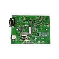
KIT PROGRAMMERS MICROID 13.56MHZ
Manufacturer
Microchip Technology
Series
MicroID®r
Type
MicroID®r
Datasheet
1.PG103003.pdf
(22 pages)
Specifications of PG103003
Contents
Programmer, Power Supply, Cable(s) and Software
Product
RFID Kits
Lead Free Status / RoHS Status
Lead free / RoHS Compliant
For Use With/related Products
MCRF355, MCRF360
Lead Free Status / RoHS Status
Lead free / RoHS Compliant, Lead free / RoHS Compliant


MCRF355
4.0
MCRF355 is a reprogrammable device in Contact
mode. The device has 154 bits of reprogrammable
memory. It can be programmed in the following proce-
dure. (A programmer, part number PG103003, is avail-
able from Microchip). Developer kits, DV103003 and
DV103006, also include contact programmers.
4.1
Programming logic is enabled by applying power to the
device and clocking the device via the CLK pad while
loading the mode code via the V
Examples 4-1 through 4-4 for test definitions). Both the
CLK and the V
resistors.
4.2
Connect antenna A, antenna B and V
ground.
4.3
1.
2.
EXAMPLE 4-1:
EXAMPLE 4-2:
DS21287G-page 10
CLK Number:
V
Apply V
V
Load mode code into the V
is sampled at CLK low-to-high edge.
CLK Number:
CLK
V
CLK:
Note: Pulsing V
Note: Erases entire array to a ‘1’ state between CLK 11 and 12.
PRG
PRG
PRG
DEVICE PROGRAMMING
Programming Logic
Pin Configuration
Pin Timing
:
:
at ground.
DDT
V
V
voltage to V
V
HH
IL
PRG
IL
V
HH
PRG
…
PROGRAMMING MODE 1: ERASE EE
PROGRAMMING MODE 2: PROGRAM EE
pads have internal pull-down
to V
1
1
HH
V
DD
V
IH
IH
for the bit programming time while holding the CLK low programs the bit to a ‘0’.
2
. Leave V
2
PRG
…
pad. The V
3
5
PRG
SS
SS
, CLK and
4
pad (See
6
pads to
PRG
5
7
Pulse high to program bit to “0”
Leave low to leave bit at “1”
6
8
3.
4.
5.
6.
4.4
4.5
Examples 4-1 through 4-4 show the timing sequence
for programming and reading of the device.
7
9
The above mode function (3.2.2) will be
executed when the last bit of code is entered.
Power the device off (V
Programming mode.
An alternative method to exit the Programming
mode is to bring CLK logic “High” before V
V
Any Programming mode can be entered after
exiting the current function.
1.
2.
3.
HH
Note:
8
10
Programming Mode
Signal Timing
(high voltage).
Erase EE Code:
Program EE Code:
Read EE Code:
9
11
Program bit #0 … Program bit #153
‘0’ means logic “Low” (V
means logic “High” (V
10
T
WC
© 2005 Microchip Technology Inc.
11
…
DD
T
WC
T
= V
0111010100
0111010010
0111010110
WC
IH
).
SS
IL
) to exit
12
) and ‘1’
165
PRG
to
Related parts for PG103003
Image
Part Number
Description
Manufacturer
Datasheet
Request
R

Part Number:
Description:
Manufacturer:
Microchip Technology Inc.
Datasheet:
Part Number:
Description:
Manufacturer:
Microchip Technology Inc.
Datasheet:
Part Number:
Description:
Manufacturer:
Microchip Technology Inc.
Datasheet:
Part Number:
Description:
Manufacturer:
Microchip Technology Inc.
Datasheet:
Part Number:
Description:
Manufacturer:
Microchip Technology Inc.
Datasheet:
Part Number:
Description:
Manufacturer:
Microchip Technology Inc.
Datasheet:
Part Number:
Description:
Manufacturer:
Microchip Technology Inc.
Datasheet:
Part Number:
Description:
Manufacturer:
Microchip Technology Inc.
Datasheet: