PG103003 Microchip Technology, PG103003 Datasheet - Page 7
PG103003
Manufacturer Part Number
PG103003
Description
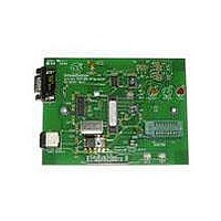
KIT PROGRAMMERS MICROID 13.56MHZ
Manufacturer
Microchip Technology
Series
MicroID®r
Type
MicroID®r
Datasheet
1.PG103003.pdf
(22 pages)
Specifications of PG103003
Contents
Programmer, Power Supply, Cable(s) and Software
Product
RFID Kits
Lead Free Status / RoHS Status
Lead free / RoHS Compliant
For Use With/related Products
MCRF355, MCRF360
Lead Free Status / RoHS Status
Lead free / RoHS Compliant, Lead free / RoHS Compliant


2.0
The device contains three major sections: (1) analog
front-end, (2) controller logic and (3) memory.
Figure 2-1 shows the block diagram of the device.
2.1
This section includes power supply, Power-on Reset,
and data modulation circuits.
2.1.1
The power supply circuit generates DC voltage (V
by rectifying induced RF coil voltage. The power supply
circuit includes high-voltage clamping diodes to
prevent excessive voltage development across the
antenna coil.
2.1.2
This circuit generates a Power-on Reset when the tag
first enters the reader field. The RESET releases when
sufficient power has developed on the V
allow for correct operation.
FIGURE 2-1:
© 2005 Microchip Technology Inc.
ANALOG FRONT-END SECTION
V
PRG
Power-on Reset
Power Supply
FUNCTIONAL DESCRIPTION
Analog Front-End Section
Modulation
and CLK
POWER SUPPLY
POWER-ON-RESET (POR)
BLOCK DIAGRAM
POR
V
DD
Modulation
Pulse
CONTROLLER LOGIC SECTION
CONTROLLER LOGIC SECTION
DD
regulator to
Column and Row Decoders
Modulation Logic
Read/Write Logic
Read/Write Logic
Clock Generator
SLEEP Timer
(anti-collision)
Test Logic
Test Logic
DD
)
2.1.3
The data modulation circuit consists of a modulation
transistor and an external LC resonant circuit. The
external circuit must be tuned to the carrier frequency
of the reader (i.e., 13.56 MHz) for maximum perfor-
mance.
The modulation transistor is placed between antenna B
and Vss pads and has small turn-on resistance (R
This small turn-on resistance shorts the external circuit
between the antenna B and Vss pads as it turns on.
The transistor turns on during the “Hi” period of the
modulation data and turns off during the “Lo” period.
When the transistor is turned off, the resonant circuit
resonates at the carrier frequency. Therefore, the
external circuit develops maximum voltage across it.
This condition is called uncloaking (tuned). When the
transistor is turned on, its low turn-on resistance shorts
the external circuit, and therefore the circuit no longer
resonates at the carrier frequency. The voltage across
the external circuit is minimized. This condition is called
cloaking (detuned).
The device transmits data by cloaking and uncloaking
based on the on/off condition of the modulation transis-
tor. Therefore, with the 70 kHz - Manchester format, the
data bit “0” will be sent by cloaking (detuned) and
uncloaking (tuned) the device for 7 s each. Similarly,
the data bit “1” will be sent by uncloaking (tuned) and
cloaking (detuned) the device for 7 s each. See
Figure 2-2 for the Manchester waveform.
CLK Pulse
Wake-up Signal
Address
Set/Clear
DATA MODULATION
Data
(High-Voltage Circuit)
MEMORY SECTION
MEMORY SECTION
Column Drivers
MCRF355
Memory Array
154-Bit
DS21287G-page 7
M
).
Related parts for PG103003
Image
Part Number
Description
Manufacturer
Datasheet
Request
R

Part Number:
Description:
Manufacturer:
Microchip Technology Inc.
Datasheet:
Part Number:
Description:
Manufacturer:
Microchip Technology Inc.
Datasheet:
Part Number:
Description:
Manufacturer:
Microchip Technology Inc.
Datasheet:
Part Number:
Description:
Manufacturer:
Microchip Technology Inc.
Datasheet:
Part Number:
Description:
Manufacturer:
Microchip Technology Inc.
Datasheet:
Part Number:
Description:
Manufacturer:
Microchip Technology Inc.
Datasheet:
Part Number:
Description:
Manufacturer:
Microchip Technology Inc.
Datasheet:
Part Number:
Description:
Manufacturer:
Microchip Technology Inc.
Datasheet: