0402ZD104KAT2A AVX Corporation, 0402ZD104KAT2A Datasheet - Page 15
0402ZD104KAT2A
Manufacturer Part Number
0402ZD104KAT2A
Description
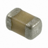
CAP CERM .1UF 10% 10V X5R 0402
Manufacturer
AVX Corporation
Series
0402r
Datasheets
1.0603ZD105KAT2A.pdf
(3 pages)
2.0402ZD104KAT2A.pdf
(3 pages)
3.0402ZD104KAT2A.pdf
(18 pages)
Specifications of 0402ZD104KAT2A
Capacitance
0.1µF
Package / Case
0402 (1005 Metric)
Voltage - Rated
10V
Tolerance
±10%
Temperature Coefficient
X5R
Mounting Type
Surface Mount, MLCC
Operating Temperature
-55°C ~ 85°C
Applications
General Purpose
Size / Dimension
0.039" L x 0.020" W (1.00mm x 0.50mm)
Thickness
0.56mm Max
Tolerance (+ Or -)
10%
Voltage
10VDC
Temp Coeff (dielectric)
X5R
Operating Temp Range
-55C to 85C
Mounting Style
Surface Mount
Construction
SMT Chip
Case Style
Ceramic Chip
Failure Rate
Not Required
Wire Form
Not Required
Product Length (mm)
1mm
Product Depth (mm)
0.5mm
Product Height (mm)
0.56mm
Product Diameter (mm)
Not Requiredmm
Dielectric Characteristic
X5R
Capacitance Tolerance
± 10%
Voltage Rating
10VDC
Capacitor Case Style
0402
No. Of Pins
2
Capacitor Mounting
SMD
Rohs Compliant
Yes
Case Size
0402
Dielectric Strength
No breakdown or visual defects
Dissipation Factor
5 %
Dissipation Factor, Test Condition
(Max.)
Insulation Resistance
100000 Megohms
Length
0.040 in. ±0.004 in.
Material, Element
Ceramic
Package Type
7 in. Reel
Temperature, Operating, Maximum
+125 °C
Temperature, Operating, Minimum
-55 °C
Termination
SMT
Voltage, Rating
10 VDC
Width
0.020 in. ±0.004 in.
Operating Temperature Range
- 55 C to + 85 C
Temperature Coefficient / Code
X5R
Product
General Type MLCCs
Dimensions
0.5 mm W x 1 mm L x 0.56 mm H
Dissipation Factor Df
5
Termination Style
SMD/SMT
Lead Free Status / RoHS Status
Lead free / RoHS Compliant
Features
-
Ratings
-
Lead Spacing
-
Lead Free Status / Rohs Status
RoHS Compliant part
Other names
478-1129-2


Surface Mounting Guide
MLC Chip Capacitors
REFLOW SOLDERING
Component pads should be designed to achieve good
solder filets and minimize component movement during
reflow soldering. Pad designs are given below for the most
common sizes of multilayer ceramic capacitors for both
wave and reflow soldering. The basis of these designs is:
WAVE SOLDERING
Component Spacing
For wave soldering components, must be spaced sufficiently
far apart to avoid bridging or shadowing (inability of solder
to penetrate properly into small spaces). This is less impor-
tant for reflow soldering but sufficient space must be
allowed to enable rework should it be required.
Component Pad Design
70
Dimensions in millimeters (inches)
D1
D1
D2
D3
D4
D2
D3
D4
D5
≥1.5mm (0.06)
≥1mm (0.04)
≥1mm (0.04)
D5
Dimensions in millimeters (inches)
Case Size
Case Size
0402
0603
0805
1206
1210
1808
1812
1825
2220
2225
0603
0805
1206
1.70 (0.07)
2.30 (0.09)
3.00 (0.12)
4.00 (0.16)
4.00 (0.16)
5.60 (0.22)
5.60 (0.22)
5.60 (0.22)
6.60 (0.26)
6.60 (0.26)
3.10 (0.12)
4.00 (0.15)
5.00 (0.19)
D1
D1
1.00 (0.04))
0.60 (0.02)
0.80 (0.03)
1.00 (0.04)
1.00 (0.04)
1.00 (0.04)
1.00 (0.04)
1.00 (0.04)
1.00 (0.04)
1.00 (0.04)
1.20 (0.05)
1.50 (0.06)
1.50 (0.06)
• Pad width equal to component width. It is permissible to
• Pad overlap 0.5mm beneath component.
• Pad extension 0.5mm beyond components for reflow and
Preheat & Soldering
The rate of preheat should not exceed 4°C/second to
prevent thermal shock. A better maximum figure is about
2°C/second.
For capacitors size 1206 and below, with a maximum
thickness of 1.25mm, it is generally permissible to allow a
temperature differential from preheat to soldering of 150°C.
In all other cases this differential should not exceed 100°C.
For further specific application or process advice, please
consult AVX.
Cleaning
Care should be taken to ensure that the capacitors are
thoroughly cleaned of flux residues especially the space
beneath the capacitor. Such residues may otherwise
become conductive and effectively offer a low resistance
bypass to the capacitor.
Ultrasonic cleaning is permissible, the recommended
conditions being 8 Watts/litre at 20-45 kHz, with a process
cycle of 2 minutes vapor rinse, 2 minutes immersion in the
ultrasonic solvent bath and finally 2 minutes vapor rinse.
D2
D2
decrease this to as low as 85% of component width but it
is not advisable to go below this.
1.0mm for wave soldering.
0.50 (0.02)
0.70 (0.03)
1.00 (0.04)
2.00 (0.09)
2.00 (0.09)
3.60 (0.14)
3.60 (0.14)
4.60 (0.18)
4.60 (0.18)
0.70 (0.03)
1.00 (0.04)
2.00 (0.09)
3.60 (0.14)
D3
D3
0.60 (0.02)
0.80 (0.03)
1.00 (0.04)
1.00 (0.04)
1.00 (0.04)
1.00 (0.04)
1.00 (0.04)
1.00 (0.04)
1.00 (0.04)
1.00 (0.04)
1.20 (0.05)
1.50 (0.06)
1.50 (0.06)
D4
D4
0.50 (0.02)
0.75 (0.03)
1.25 (0.05)
1.60 (0.06)
2.50 (0.10)
2.00 (0.08)
3.00 (0.12)
6.35 (0.25)
5.00 (0.20)
6.35 (0.25)
0.75 (0.03)
1.25 (0.05)
1.60 (0.06)
D5
D5
Related parts for 0402ZD104KAT2A
Image
Part Number
Description
Manufacturer
Datasheet
Request
R

Part Number:
Description:
Manufacturer:
AVX Corporation
Datasheet:
Part Number:
Description:
Manufacturer:
AVX Corporation
Datasheet:
Part Number:
Description:
Manufacturer:
AVX Corporation
Datasheet:
Part Number:
Description:
Manufacturer:
AVX Corporation
Datasheet:
Part Number:
Description:
Manufacturer:
AVX Corporation
Datasheet: