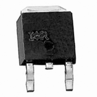
IRFR18N15D International Rectifier, IRFR18N15D Datasheet

IRFR18N15D
Specifications of IRFR18N15D
Available stocks
Related parts for IRFR18N15D
IRFR18N15D Summary of contents
Page 1
... Telecom 48V input DC-DC Active Clamp Reset Forward Converter Notes through are on page 10 www.irf.com SMPS MOSFET HEXFET V DSS 150V D-Pak IRFR18N15D @ 10V GS @ 10V GS - 175 300 (1.6mm from case ) PD- 93815A IRFR18N15D IRFU18N15D ® Power MOSFET R max I DS(on) D 0.125 18A I-Pak IRFU18N15D Max. Units ...
Page 2
... IRFR18N15D/IRFU18N15D Static @ T = 25°C (unless otherwise specified) J Parameter V Drain-to-Source Breakdown Voltage (BR)DSS Breakdown Voltage Temp. Coefficient (BR)DSS J R Static Drain-to-Source On-Resistance DS(on) V Gate Threshold Voltage GS(th) I Drain-to-Source Leakage Current DSS Gate-to-Source Forward Leakage I GSS Gate-to-Source Reverse Leakage Dynamic @ T = 25°C (unless otherwise specified) ...
Page 3
... Drain-to-Source Voltage (V) DS Fig 1. Typical Output Characteristics 100 ° 175 ° 20µs PULSE WIDTH Gate-to-Source Voltage (V) GS Fig 3. Typical Transfer Characteristics www.irf.com IRFR18N15D/IRFU18N15D 100 TOP BOTTOM 10 ° 1 0.1 10 100 Fig 2. Typical Output Characteristics 3 2.5 2.0 1.5 1.0 0.5 = 50V 0.0 -60 -40 - Fig 4 ...
Page 4
... IRFR18N15D/IRFU18N15D 10000 0V, C iss = rss = oss = 1000 Ciss Coss 100 Crss Drain-to-Source Voltage (V) Fig 5. Typical Capacitance Vs. Drain-to-Source Voltage 100 10 ° 175 0.1 0.2 0.5 0.8 V ,Source-to-Drain Voltage (V) SD Fig 7. Typical Source-Drain Diode Forward Voltage MHZ SHORTED 100 1000 0 0 Fig 6. Typical Gate Charge Vs. ...
Page 5
... Case Temperature 0.50 0.20 0.10 0.05 0.1 0.02 SINGLE PULSE 0.01 (THERMAL RESPONSE) 0.01 0.00001 0.0001 Fig 11. Maximum Effective Transient Thermal Impedance, Junction-to-Case www.irf.com IRFR18N15D/IRFU18N15D R G Pulse Width Duty Factor Fig 10a. Switching Time Test Circuit V DS 90% 150 175 ° 10 d(on) Fig 10b ...
Page 6
... IRFR18N15D/IRFU18N15D Fig 12a. Unclamped Inductive Test Circuit Fig 12b. Unclamped Inductive Waveforms Charge Fig 13a. Basic Gate Charge Waveform Current Regulator Same Type as D.U.T. 50K .2 F 12V .3 F D.U. 3mA Current Sampling Resistors Fig 13b. Gate Charge Test Circuit 6 500 400 ...
Page 7
... Current D.U.T. V Waveform DS Re-Applied Voltage Inductor Curent * for Logic Level Devices GS Fig 14. For N-Channel HEXFET www.irf.com IRFR18N15D/IRFU18N15D Peak Diode Recovery dv/dt Test Circuit + Circuit Layout Considerations Low Stray Inductance Ground Plane Low Leakage Inductance Current Transformer - - + dv/dt controlled Driver same type as D.U.T. ...
Page 8
... IRFR18N15D/IRFU18N15D D-Pak (TO-252AA) Package Outline Dimensions are shown in millimeters (inches (. (. (. (. (. (. 1 1 D-Pak (TO-252AA) Part Marking Information (. (. (. (. (. (. & (. (. (. (. (. (. (. (. (. (. www.irf.com ...
Page 9
... I-Pak (TO-251AA) Package Outline Dimensions are shown in millimeters (inches (. (. (. (. (. (. 2 1 .28 (. I-Pak (TO-251AA) Part Marking Information www.irf.com IRFR18N15D/IRFU18N15D (. (. (. (. (. (. & . 0 ...
Page 10
... IRFR18N15D/IRFU18N15D D-Pak (TO-252AA) Tape & Reel Information Dimensions are shown in millimeters (inches 12 11 LLIN G D IME ILL ILLIM -481 & - -481 . Notes: Repetitive rating; pulse width limited by max. junction temperature. Starting T = 25° 3.3mH 11A 11A, di/dt 170A/µ 175° When mounted on 1" ...
Page 11
Note: For the most current drawings please refer to the IR website at: http://www.irf.com/package/ ...


