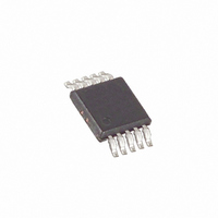
MAX3208EAUB+ Maxim Integrated Products, MAX3208EAUB+ Datasheet - Page 4

MAX3208EAUB+
Manufacturer Part Number
MAX3208EAUB+
Description
IC ESD PROT DIFF 10-UMAX
Manufacturer
Maxim Integrated Products
Type
Diode Arraysr
Series
MAX3208Er
Datasheet
1.MAX3208EAUB.pdf
(9 pages)
Specifications of MAX3208EAUB+
Power (watts)
444mW
Polarization
4 Channel Array - Unidirectional
Mounting Type
Surface Mount
Package / Case
10-MSOP, Micro10™, 10-uMAX, 10-uSOP
Capacitance Value
10(Typ) pF
Maximum Clamping Voltage
105.5 V
Number Of Elements Per Chip
4
Esd Protection Voltage
±15@HBM|±15@Air Gap|±8@Contact Disc KV
Maximum Leakage Current
0.1 uA
Channels
4 Channels
Clamping Voltage
100 V
Operating Voltage
- 0.3 V to + 6.0 V
Termination Style
SMD/SMT
Capacitance
2 pF
Maximum Operating Temperature
+ 125 C
Minimum Operating Temperature
- 40 C
Dimensions
3.05 (Max) mm W x 3.05 (Max) mm L
Diode Type
ESD Protection
Power Dissipation Pd
444mW
Diode Case Style
µMAX
No. Of Pins
10
Termination Type
SMD
Capacitance, Cd
2.6pF
Operating Temperature Range
-40°C To +125°C
Rohs Compliant
Yes
Filter Terminals
SMD
Esd Threat Voltage Max
15kV
Lead Free Status / RoHS Status
Lead free / RoHS Compliant
Voltage - Breakdown
-
Voltage - Reverse Standoff (typ)
-
Lead Free Status / Rohs Status
Lead free / RoHS Compliant
The MAX3205E/MAX3207E/MAX3208E low-capacitance,
±15kV ESD-protection diode arrays with an integrated
transient voltage suppressor (TVS) clamp are suitable for
high-speed and general-signal ESD protection. Low
input capacitance makes these devices ideal for ESD
protection of signals in HDTV, PC monitors (DVI, HDMI),
PC peripherals (FireWire, USB 2.0), server interconnect
(PCI Express, InfiniBand), datacom, and interchassis
interconnect. Each channel consists of a pair of diodes
that steer ESD current pulses to V
MAX3207E, MAX3208E, and MAX3205E are two, four,
and six channels (see the Functional Diagram ).
The MAX3205E/MAX3207E/MAX3208E are designed to
work in conjunction with a device’s intrinsic ESD pro-
tection. The MAX3205E/MAX3207E/MAX3208E limit the
Dual, Quad, and Hex High-Speed
Differential ESD-Protection ICs
4
_______________________________________________________________________________________
I/O1
MAX3207E
V
GND
CC
I/O2
Detailed Description
I/O1
I/O2
CC
or GND. The
MAX3208E
GND
V
CC
I/O3
I/O4
excursion of the ESD event to below ±25V peak voltage
when subjected to the Human Body Model waveform.
When subjected to the IEC 61000-4-2 waveform and
Contact Discharge, the peak voltage is limited to ±60V.
The peak voltage is limited to ±100V when subjected to
Air-Gap Discharge. The device protected by the
MAX3205E/MAX3207E/MAX3208E must be able to
withstand these peak voltages, plus any additional volt-
age generated by the parasitic of the board.
A TVS is integrated into the MAX3205E/MAX3207E/
MAX3208E to help clamp ESD to a known voltage. This
helps reduce the effects of parasitic inductance on the
V
ESD event. For the lowest possible clamp voltage dur-
ing an ESD event, placing a 0.1µF capacitor as close to
V
CC
CC
as possible is recommended.
rail by clamping V
I/O1
I/O2
I/O3
CC
Functional Diagram
to a known voltage during an
MAX3205E
GND
V
CC
I/O4
I/O5
I/O6


