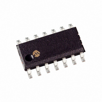
PIC16F688-I/SL Microchip Technology, PIC16F688-I/SL Datasheet - Page 107

PIC16F688-I/SL
Manufacturer Part Number
PIC16F688-I/SL
Description
IC PIC MCU FLASH 4KX14 14SOIC
Manufacturer
Microchip Technology
Series
PIC® 16Fr
Datasheets
1.PIC16F616T-ISL.pdf
(8 pages)
2.PIC16F688T-ISL.pdf
(204 pages)
3.PIC16F688T-ISL.pdf
(6 pages)
4.PIC16F688T-ISL.pdf
(4 pages)
5.PIC16F688T-ISL.pdf
(688 pages)
6.PIC16F688-EP.pdf
(174 pages)
Specifications of PIC16F688-I/SL
Program Memory Type
FLASH
Program Memory Size
7KB (4K x 14)
Package / Case
14-SOIC (3.9mm Width), 14-SOL
Core Processor
PIC
Core Size
8-Bit
Speed
20MHz
Connectivity
UART/USART
Peripherals
Brown-out Detect/Reset, POR, WDT
Number Of I /o
12
Eeprom Size
256 x 8
Ram Size
256 x 8
Voltage - Supply (vcc/vdd)
2 V ~ 5.5 V
Data Converters
A/D 8x10b
Oscillator Type
Internal
Operating Temperature
-40°C ~ 85°C
Processor Series
PIC16F
Core
PIC
Data Bus Width
8 bit
Data Ram Size
256 B
Interface Type
SCI, USART
Maximum Clock Frequency
20 MHz
Number Of Programmable I/os
12
Number Of Timers
1
Operating Supply Voltage
2 V to 5.5 V
Maximum Operating Temperature
+ 85 C
Mounting Style
SMD/SMT
3rd Party Development Tools
52715-96, 52716-328, 52717-734
Development Tools By Supplier
PG164130, DV164035, DV244005, DV164005, PG164120, ICE2000, DM163014, DM164120-4
Minimum Operating Temperature
- 40 C
On-chip Adc
8 bit
Lead Free Status / RoHS Status
Lead free / RoHS Compliant
For Use With
XLT14SO-1 - SOCKET TRANSITION 14SOIC 150/208AC162061 - HEADER INTRFC MPLAB ICD2 20PINAC162056 - HEADER INTERFACE ICD2 16F688
Lead Free Status / Rohs Status
Lead free / RoHS Compliant
Available stocks
Company
Part Number
Manufacturer
Quantity
Price
Company:
Part Number:
PIC16F688-I/SL
Manufacturer:
MICROCHIP
Quantity:
4 952
Company:
Part Number:
PIC16F688-I/SL
Manufacturer:
Microchip Technology
Quantity:
27 564
Part Number:
PIC16F688-I/SL
Manufacturer:
MICROCHIP/微芯
Quantity:
20 000
10.4.1.5
Data is received at the RX/DT pin. The RX/DT and TX/
CK pin output drivers are automatically disabled when
the EUSART is configured for synchronous master
receive operation.
In Synchronous mode, reception is enabled by setting
either the Single Receive Enable bit (SREN of the
RCSTA register) or the Continuous Receive Enable bit
(CREN of the RCSTA register).
When SREN is set and CREN is clear, only as many
clock cycles are generated as there are data bits in a
single character. The SREN bit is automatically cleared
at the completion of one character. When CREN is set,
clocks are continuously generated until CREN is
cleared. If CREN is cleared in the middle of a character
the CK clock stops immediately and the partial charac-
ter is discarded. If SREN and CREN are both set, then
SREN is cleared at the completion of the first character
and CREN takes precedence.
To initiate reception, set either SREN or CREN. Data is
sampled at the RX/DT pin on the trailing edge of the
TX/CK clock pin and is shifted into the Receive Shift
Register (RSR). When a complete character is
received into the RSR, the RCIF bit is set and the char-
acter is automatically transferred to the two character
receive FIFO. The Least Significant eight bits of the top
character in the receive FIFO are available in RCREG.
The RCIF bit remains set as long as there are un-read
characters in the receive FIFO.
10.4.1.6
The receive FIFO buffer can hold two characters. An
overrun error will be generated if a third character, in its
entirety, is received before RCREG is read to access
the FIFO. When this happens the OERR bit of the
RCSTA register is set. Previous data in the FIFO will
not be overwritten. The two characters in the FIFO
buffer can be read, however, no additional characters
will be received until the error is cleared. The OERR bit
can only be cleared by clearing the overrun condition.
If the overrun error occurred when the SREN bit is set
and CREN is clear then the error is cleared by reading
RCREG. If the overrun occurred when the CREN bit is
set then the error condition is cleared by either clearing
the CREN bit of the RCSTA register or by clearing the
SPEN bit which resets the EUSART.
10.4.1.7
The EUSART supports 9-bit character reception. When
the RX9 bit of the RCSTA register is set the EUSART
will shift 9-bits into the RSR for each character
received. The RX9D bit of the RCSTA register is the
ninth, and Most Significant, data bit of the top unread
character in the receive FIFO. When reading 9-bit data
from the receive FIFO buffer, the RX9D data bit must
be read before reading the 8 Least Significant bits from
the RCREG.
© 2009 Microchip Technology Inc.
Synchronous Master Reception
Receive Overrun Error
Receiving 9-bit Characters
10.4.1.8
1.
2.
3.
4.
5.
6.
7.
8.
9.
10. If an overrun error occurs, clear the error by
Initialize the SPBRGH, SPBRG register pair for
the appropriate baud rate. Set or clear the
BRGH and BRG16 bits, as required, to achieve
the desired baud rate.
Enable the synchronous master serial port by
setting bits SYNC, SPEN and CSRC.
Ensure bits CREN and SREN are clear.
If using interrupts, set the GIE and PEIE bits of
the INTCON register and set RCIE.
If 9-bit reception is desired, set bit RX9.
Start reception by setting the SREN bit or for
continuous reception, set the CREN bit.
Interrupt flag bit RCIF will be set when reception
of a character is complete. An interrupt will be
generated if the enable bit RCIE was set.
Read the RCSTA register to get the ninth bit (if
enabled) and determine if any error occurred
during reception.
Read the 8-bit received data by reading the
RCREG register.
either clearing the CREN bit of the RCSTA
register or by clearing the SPEN bit which resets
the EUSART.
Synchronous Master Reception Set-
up:
PIC16F688
DS41203E-page 105


