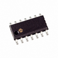
PIC16F688-I/SL Microchip Technology, PIC16F688-I/SL Datasheet - Page 417

PIC16F688-I/SL
Manufacturer Part Number
PIC16F688-I/SL
Description
IC PIC MCU FLASH 4KX14 14SOIC
Manufacturer
Microchip Technology
Series
PIC® 16Fr
Datasheets
1.PIC16F616T-ISL.pdf
(8 pages)
2.PIC16F688T-ISL.pdf
(204 pages)
3.PIC16F688T-ISL.pdf
(6 pages)
4.PIC16F688T-ISL.pdf
(4 pages)
5.PIC16F688T-ISL.pdf
(688 pages)
6.PIC16F688-EP.pdf
(174 pages)
Specifications of PIC16F688-I/SL
Program Memory Type
FLASH
Program Memory Size
7KB (4K x 14)
Package / Case
14-SOIC (3.9mm Width), 14-SOL
Core Processor
PIC
Core Size
8-Bit
Speed
20MHz
Connectivity
UART/USART
Peripherals
Brown-out Detect/Reset, POR, WDT
Number Of I /o
12
Eeprom Size
256 x 8
Ram Size
256 x 8
Voltage - Supply (vcc/vdd)
2 V ~ 5.5 V
Data Converters
A/D 8x10b
Oscillator Type
Internal
Operating Temperature
-40°C ~ 85°C
Processor Series
PIC16F
Core
PIC
Data Bus Width
8 bit
Data Ram Size
256 B
Interface Type
SCI, USART
Maximum Clock Frequency
20 MHz
Number Of Programmable I/os
12
Number Of Timers
1
Operating Supply Voltage
2 V to 5.5 V
Maximum Operating Temperature
+ 85 C
Mounting Style
SMD/SMT
3rd Party Development Tools
52715-96, 52716-328, 52717-734
Development Tools By Supplier
PG164130, DV164035, DV244005, DV164005, PG164120, ICE2000, DM163014, DM164120-4
Minimum Operating Temperature
- 40 C
On-chip Adc
8 bit
Lead Free Status / RoHS Status
Lead free / RoHS Compliant
For Use With
XLT14SO-1 - SOCKET TRANSITION 14SOIC 150/208AC162061 - HEADER INTRFC MPLAB ICD2 20PINAC162056 - HEADER INTERFACE ICD2 16F688
Lead Free Status / Rohs Status
Lead free / RoHS Compliant
Available stocks
Company
Part Number
Manufacturer
Quantity
Price
Company:
Part Number:
PIC16F688-I/SL
Manufacturer:
MICROCHIP
Quantity:
4 952
Company:
Part Number:
PIC16F688-I/SL
Manufacturer:
Microchip Technology
Quantity:
27 564
Part Number:
PIC16F688-I/SL
Manufacturer:
MICROCHIP/微芯
Quantity:
20 000
- PIC16F616T-ISL PDF datasheet
- PIC16F688T-ISL PDF datasheet #2
- PIC16F688T-ISL PDF datasheet #3
- PIC16F688T-ISL PDF datasheet #4
- PIC16F688T-ISL PDF datasheet #5
- PIC16F688-EP PDF datasheet #6
- Current page: 417 of 688
- Download datasheet (3Mb)
Section 22. Basic 8-bit A/D Converter
22.8
A/D Accuracy/Error
In systems where the device frequency is low, use of the A/D RC clock is preferred. At moderate
to high frequencies, T
should be derived from the device oscillator.
AD
The absolute accuracy specified for the A/D converter includes the sum of all contributions for
quantization error, integral error, differential error, full scale error, offset error, and monotonicity.
It is defined as the maximum deviation from an actual transition versus an ideal transition for any
code. The absolute error of the A/D converter is specified at < 1 LSb for V
= V
(over the
DD
REF
device’s specified operating range). However, the accuracy of the A/D converter will degrade as
V
diverges from V
.
DD
REF
For a given range of analog inputs, the output digital code will be the same. This is due to the
quantization of the analog input to a digital code. Quantization error is typically
1/2 LSb and is
22
inherent in the analog to digital conversion process. The only way to reduce quantization error is
to increase the resolution of the A/D converter.
Offset error measures the first actual transition of a code versus the first ideal transition of a code.
Offset error shifts the entire transfer function. Offset error can be calibrated out of a system or
introduced into a system through the interaction of the total leakage current and source imped-
ance at the analog input.
Gain error measures the maximum deviation of the last actual transition and the last ideal tran-
sition adjusted for offset error. This error appears as a change in slope of the transfer function.
The difference in gain error to full scale error is that full scale does not take offset error into
account. Gain error can be calibrated out in software.
Linearity error refers to the uniformity of the code changes. Linearity errors cannot be calibrated
out of the system. Integral non-linearity error measures the actual code transition versus the ideal
code transition adjusted by the gain error for each code.
Differential non-linearity measures the maximum actual code width versus the ideal code width.
This measure is unadjusted.
The maximum pin leakage current is specified in the Device Data Sheet electrical specification
parameter
D060.
In systems where the device frequency is low, use of the A/D RC clock is preferred. At moderate
to high frequencies, T
should be derived from the device oscillator. T
must not violate the
AD
AD
minimum and should be minimized to reduce inaccuracies due to noise and sampling capacitor
bleed off.
In systems where the device will enter SLEEP mode after the start of the A/D conversion, the RC
clock source selection is required. In this mode, the digital noise from the modules in SLEEP are
stopped. This method gives high accuracy.
1997 Microchip Technology Inc.
DS31022A-page 22-15
Related parts for PIC16F688-I/SL
Image
Part Number
Description
Manufacturer
Datasheet
Request
R

Part Number:
Description:
Manufacturer:
Microchip Technology Inc.
Datasheet:

Part Number:
Description:
IC MCU FLASH 4KX14 14TSSOP
Manufacturer:
Microchip Technology
Datasheet:

Part Number:
Description:
IC PIC MCU FLASH 4KX14 14DIP
Manufacturer:
Microchip Technology
Datasheet:

Part Number:
Description:
IC PIC MCU FLASH 4KX14 16QFN
Manufacturer:
Microchip Technology
Datasheet:

Part Number:
Description:
IC MCU PIC FLASH 4KX14 14SOIC
Manufacturer:
Microchip Technology
Datasheet:

Part Number:
Description:
IC PIC MCU FLASH 4KX14 14TSSOP
Manufacturer:
Microchip Technology
Datasheet:

Part Number:
Description:
IC MCU PIC FLASH 4KX14 14DIP
Manufacturer:
Microchip Technology
Datasheet:

Part Number:
Description:
IC PIC MCU FLASH 4KX14 16QFN
Manufacturer:
Microchip Technology
Datasheet:

Part Number:
Description:
IC PIC MCU FLASH 4KX14 14TSSOP
Manufacturer:
Microchip Technology
Datasheet:

Part Number:
Description:
IC, 8BIT MCU, PIC16F, 32MHZ, SOIC-18
Manufacturer:
Microchip Technology
Datasheet:

Part Number:
Description:
IC, 8BIT MCU, PIC16F, 32MHZ, SSOP-20
Manufacturer:
Microchip Technology
Datasheet:

Part Number:
Description:
IC, 8BIT MCU, PIC16F, 32MHZ, DIP-18
Manufacturer:
Microchip Technology
Datasheet:

Part Number:
Description:
IC, 8BIT MCU, PIC16F, 32MHZ, QFN-28
Manufacturer:
Microchip Technology
Datasheet:

Part Number:
Description:
IC, 8BIT MCU, PIC16F, 32MHZ, QFN-28
Manufacturer:
Microchip Technology
Datasheet:

Part Number:
Description:
IC, 8BIT MCU, PIC16F, 32MHZ, QFN-28
Manufacturer:
Microchip Technology
Datasheet:


