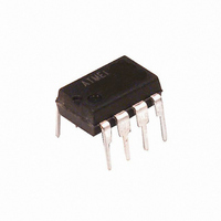
ATTINY25-20PU Atmel, ATTINY25-20PU Datasheet - Page 160

ATTINY25-20PU
Manufacturer Part Number
ATTINY25-20PU
Description
IC AVR MCU 2K 20MHZ 8-DIP
Manufacturer
Atmel
Series
AVR® ATtinyr
Specifications of ATTINY25-20PU
Core Processor
AVR
Core Size
8-Bit
Speed
20MHz
Connectivity
USI
Peripherals
Brown-out Detect/Reset, POR, PWM, WDT
Number Of I /o
6
Program Memory Size
2KB (1K x 16)
Program Memory Type
FLASH
Eeprom Size
128 x 8
Ram Size
128 x 8
Voltage - Supply (vcc/vdd)
2.7 V ~ 5.5 V
Data Converters
A/D 4x10b
Oscillator Type
Internal
Operating Temperature
-40°C ~ 85°C
Package / Case
8-DIP (0.300", 7.62mm)
Processor Series
ATTINY2x
Core
AVR8
Data Bus Width
8 bit
Data Ram Size
128 B
Interface Type
USI
Maximum Clock Frequency
10 MHz
Number Of Programmable I/os
6
Number Of Timers
2
Operating Supply Voltage
2.7 V to 5.5 V
Maximum Operating Temperature
+ 85 C
Mounting Style
Through Hole
3rd Party Development Tools
EWAVR, EWAVR-BL
Development Tools By Supplier
ATAVRDRAGON, ATSTK500, ATSTK600, ATAVRISP2, ATAVRONEKIT
Minimum Operating Temperature
- 40 C
On-chip Adc
10 bit, 4 Channel
Data Rom Size
128 B
A/d Bit Size
10 bit
A/d Channels Available
4
Height
3.3 mm
Length
9.27 mm
Supply Voltage (max)
5.5 V
Supply Voltage (min)
2.7 V
Width
6.35 mm
For Use With
ATSTK600-DIP40 - STK600 SOCKET/ADAPTER 40-PDIPATAVRBC100 - REF DESIGN KIT BATTERY CHARGER770-1007 - ISP 4PORT ATMEL AVR MCU SPI/JTAGATAVRDRAGON - KIT DRAGON 32KB FLASH MEM AVRATAVRISP2 - PROGRAMMER AVR IN SYSTEMATJTAGICE2 - AVR ON-CHIP D-BUG SYSTEM
Lead Free Status / RoHS Status
Lead free / RoHS Compliant
- Current page: 160 of 236
- Download datasheet (5Mb)
20.7.2
20.7.3
160
ATtiny25/45/85
Considerations for Efficient Programming
Chip Erase
If the rise time of the V
tive algorithm can be used:
Table 20-15. High-voltage Reset Characteristics
The loaded command and address are retained in the device during programming. For efficient
programming, the following should be considered.
The Chip Erase will erase the Flash and EEPROM
not reset until the Program memory has been completely erased. The Fuse bits are not
Supply Voltage
V
4.5V
5.5V
3. Wait 20 - 60 µs, and apply 11.5 - 12.5V to RESET.
4. Keep the Prog_enable pins unchanged for at least 10 µs after the High-voltage has
5. Release the Prog_enable[2] pin to avoid drive contention on the Prog_enable[2]/SDO
6. Wait at least 300 µs before giving any serial instructions on SDI/SII.
7. Exit Programming mode by power the device down or by bringing RESET pin to 0V.
1. Set Prog_enable pins listed in
2. Apply 4.5 - 5.5V between V
3. Monitor V
4. Keep the Prog_enable pins unchanged for at least 10 µs after the High-voltage has
5. Release the Prog_enable[2] pin to avoid drive contention on the Prog_enable[2]/SDO
6. Wait until V
7. Exit Programming mode by power the device down or by bringing RESET pin to 0V.
• The command needs only be loaded once when writing or reading multiple memory
• Skip writing the data value 0xFF that is the contents of the entire EEPROM (unless the
• Address High byte needs only be loaded before programming or reading a new 256 word
CC
locations.
EESAVE Fuse is programmed) and Flash after a Chip Erase.
window in Flash or 256 byte EEPROM. This consideration also applies to Signature bytes
reading.
been applied to ensure the Prog_enable Signature has been latched.
pin.
been applied to ensure the Prog_enable Signature has been latched.
pin.
SDI/SII.
CC
CC
, and as soon as V
actually reaches 4.5 - 5.5V before giving any serial instructions on
RESET Pin High-voltage Threshold
CC
is unable to fulfill the requirements listed above, the following alterna-
CC
V
and GND.
Table 20-14
11.5V
11.5V
CC
HVRST
reaches 0.9 - 1.1V, apply 11.5 - 12.5V to RESET.
to “000”, RESET pin and V
(1)
memories plus Lock bits. The Lock bits are
Minimum High-voltage Period for
Latching Prog_enable
t
100 ns
100 ns
HVRST
CC
to 0V.
2586M–AVR–07/10
Related parts for ATTINY25-20PU
Image
Part Number
Description
Manufacturer
Datasheet
Request
R

Part Number:
Description:
Manufacturer:
Atmel Corporation
Datasheet:

Part Number:
Description:
Manufacturer:
Atmel Corporation
Datasheet:

Part Number:
Description:
IC MCU AVR 2K FLASH 20MHZ 20-QFN
Manufacturer:
Atmel
Datasheet:

Part Number:
Description:
IC AVR MCU 2K 20MHZ 8-SOIC
Manufacturer:
Atmel
Datasheet:

Part Number:
Description:
MCU AVR 2K FLASH 15MHZ 20-QFN
Manufacturer:
Atmel
Datasheet:

Part Number:
Description:
8-bit Microcontrollers - MCU AVR 16KB FL 512B EE 1KB SRAM 10 MHZ GRN
Manufacturer:
Atmel

Part Number:
Description:
8-bit Microcontrollers - MCU AVR 16KB FL 512B EE 1KB SRAM 10 MHZ GRN
Manufacturer:
Atmel

Part Number:
Description:
MCU AVR 2K ISP FLASH 2.7V 8-SOIC
Manufacturer:
Atmel
Datasheet:

Part Number:
Description:
MCU AVR 2KB FLASH 20MHZ 8SOIC
Manufacturer:
Atmel
Datasheet:

Part Number:
Description:
IC MCU AVR 2KB FLASH 20MHZ 8SOIC
Manufacturer:
Atmel
Datasheet:

Part Number:
Description:
IC MCU AVR 2KB FLASH 20MHZ 8SOIC
Manufacturer:
Atmel
Datasheet:

Part Number:
Description:
MCU AVR 2KB FLASH 20MHZ 8SOIC
Manufacturer:
Atmel
Datasheet:

Part Number:
Description:
MCU AVR 2KB FLASH 20MHZ 8SOIC
Manufacturer:
Atmel
Datasheet:

Part Number:
Description:
MCU AVR 2KB FLASH 20MHZ 20QFN
Manufacturer:
Atmel
Datasheet:


