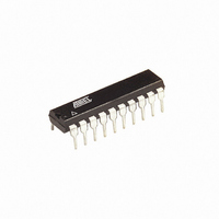
AT89LP2052-20PU Atmel, AT89LP2052-20PU Datasheet - Page 74

AT89LP2052-20PU
Manufacturer Part Number
AT89LP2052-20PU
Description
IC 8051 MCU FLASH 2K 20DIP
Manufacturer
Atmel
Series
89LPr
Datasheet
1.AT89LP2052-20PU.pdf
(94 pages)
Specifications of AT89LP2052-20PU
Core Processor
8051
Core Size
8-Bit
Speed
20MHz
Connectivity
SPI, UART/USART
Peripherals
Brown-out Detect/Reset, POR, PWM, WDT
Number Of I /o
15
Program Memory Size
2KB (2K x 8)
Program Memory Type
FLASH
Ram Size
256 x 8
Voltage - Supply (vcc/vdd)
2.4 V ~ 5.5 V
Oscillator Type
Internal
Operating Temperature
-40°C ~ 85°C
Package / Case
20-DIP (0.300", 7.62mm)
Processor Series
AT89x
Core
8051
Data Bus Width
8 bit
Data Ram Size
256 B
Interface Type
SPI/UART
Maximum Clock Frequency
20 MHz
Number Of Programmable I/os
15
Number Of Timers
2
Operating Supply Voltage
2.4 V to 5.5 V
Maximum Operating Temperature
+ 85 C
Mounting Style
Through Hole
3rd Party Development Tools
PK51, CA51, A51, ULINK2
Development Tools By Supplier
AT89ISP
Minimum Operating Temperature
- 40 C
Package
20PDIP
Device Core
8051
Family Name
AT89
Maximum Speed
20 MHz
Cpu Family
AT89
Device Core Size
8b
Frequency (max)
20MHz
Total Internal Ram Size
256Byte
# I/os (max)
15
Number Of Timers - General Purpose
2
Operating Supply Voltage (typ)
2.5/3.3/5V
Operating Supply Voltage (max)
5.5V
Operating Supply Voltage (min)
2.4V
Instruction Set Architecture
CISC
Operating Temp Range
-40C to 85C
Operating Temperature Classification
Industrial
Mounting
Through Hole
Pin Count
20
Package Type
PDIP
Lead Free Status / RoHS Status
Lead free / RoHS Compliant
Eeprom Size
-
Data Converters
-
Lead Free Status / Rohs Status
Lead free / RoHS Compliant
Available stocks
Company
Part Number
Manufacturer
Quantity
Price
Company:
Part Number:
AT89LP2052-20PU
Manufacturer:
ON
Quantity:
340
23.5.1
74
AT89LP2052/LP4052
Power-up Sequence
Figure 23-21. ISP/Serial Programming Device Connections
Note:
Execute this sequence to power-up the device before serial programming.
Figure 23-22. Serial Programming Power-up Sequence
1. Apply power between VCC and GND pins.
2. Keep SCK (P1.7) and SS (P1.4) at “L”.
3. Wait 10 µs and bring RST and SS to “H”.
4. Wait at least 2 ms for internal Power-on Reset to time out.
SCK frequency should be less than 5 MHz.
MISO
MOSI
RST
SCK
V
SS
CC
Serial Clock
Serial Out
Se rial In
CS
P1.7/SCK
P1.6/MISO
P1.5/MOSI
P1.4/SS
GND
AT89LP2052/LP4052
HIGH Z
HIGH Z
VCC
RST
2.7 to 5.5V
V IH
3547J–MICRO–10/09


