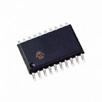
PIC18LF13K22-I/SO Microchip Technology, PIC18LF13K22-I/SO Datasheet - Page 143

PIC18LF13K22-I/SO
Manufacturer Part Number
PIC18LF13K22-I/SO
Description
IC PIC MCU FLASH 256KX8 20-SOIC
Manufacturer
Microchip Technology
Series
PIC® XLP™ 18Fr
Datasheets
1.PIC18LF13K22-ISS.pdf
(388 pages)
2.PIC18LF13K22-ISS.pdf
(12 pages)
3.PIC18LF13K22-ISS.pdf
(36 pages)
4.PIC18LF14K22-IP.pdf
(382 pages)
Specifications of PIC18LF13K22-I/SO
Program Memory Type
FLASH
Program Memory Size
8KB (4K x 16)
Package / Case
20-SOIC (7.5mm Width)
Core Processor
PIC
Core Size
8-Bit
Speed
64MHz
Connectivity
I²C, LIN, SPI, UART/USART
Peripherals
Brown-out Detect/Reset, POR, PWM, WDT
Number Of I /o
17
Eeprom Size
256 x 8
Ram Size
256 x 8
Voltage - Supply (vcc/vdd)
1.8 V ~ 3.6 V
Data Converters
A/D 12x10b
Oscillator Type
Internal
Operating Temperature
-40°C ~ 85°C
Processor Series
PIC18LF
Core
PIC
Data Bus Width
8 bit
Data Ram Size
256 B
Interface Type
I2C, MSSP, SPI, USART
Maximum Clock Frequency
32 KHz
Number Of Programmable I/os
18
Number Of Timers
4
Operating Supply Voltage
1.8 V to 3.6 V
Maximum Operating Temperature
+ 125 C
Mounting Style
SMD/SMT
3rd Party Development Tools
52715-96, 52716-328, 52717-734, 52712-325, EWPIC18
Development Tools By Supplier
PG164130, DV164035, DV244005, DV164005
Minimum Operating Temperature
- 40 C
On-chip Adc
10 bit, 12 Channel
Lead Free Status / RoHS Status
Lead free / RoHS Compliant
Lead Free Status / RoHS Status
Lead free / RoHS Compliant, Lead free / RoHS Compliant
- PIC18LF13K22-ISS PDF datasheet
- PIC18LF13K22-ISS PDF datasheet #2
- PIC18LF13K22-ISS PDF datasheet #3
- PIC18LF14K22-IP PDF datasheet #4
- Current page: 143 of 388
- Download datasheet (4Mb)
14.2.8
In SPI Master mode, module clocks may be operating
at a different speed than when in Full Power mode; in
the case of the Sleep mode, all clocks are halted.
In all Idle modes, a clock is provided to the peripherals.
That clock could be from the primary clock source, the
secondary clock (Timer1 oscillator at 32.768 kHz) or
the INTOSC source. See Section 18.0 “Power-Man-
aged Modes” for additional information.
In most cases, the speed that the master clocks SPI
data is not important; however, this should be
evaluated for each system.
When MSSP interrupts are enabled, after the master
completes sending data, an MSSP interrupt will wake
the controller:
• from Sleep, in Slave mode
• from Idle, in Slave or Master mode
If an exit from Sleep or Idle mode is not desired, MSSP
interrupts should be disabled.
In SPI Master mode, when the Sleep mode is selected,
all module clocks are halted and the transmis-
sion/reception will remain in that state until the device
wakes. After the device returns to Run mode, the mod-
ule will resume transmitting and receiving data.
In SPI Slave mode, the SPI Transmit/Receive Shift
register operates asynchronously to the device. This
allows the device to be placed in any Power-Managed
mode
TABLE 14-2:
2010 Microchip Technology Inc.
INTCON
IPR1
PIE1
PIR1
TRISB
TRISC
SSPBUF
SSPCON1
SSPSTAT
Legend: Shaded cells are not used by the MSSP in SPI mode.
Name
and
OPERATION IN POWER-MANAGED
MODES
SSP Receive Buffer/Transmit Register
data
GIE/GIEH PEIE/GIEL TMR0IE
TRISC7
TRISB7
WCOL
Bit 7
SMP
REGISTERS ASSOCIATED WITH SPI OPERATION
—
—
—
to be
TRISB6
TRISC6
SSPOV
ADIP
ADIE
Bit 6
ADIF
CKE
shifted into
TRISB5
TRISC5
SSPEN
RCIP
RCIE
RCIF
Bit 5
D/A
the
TRISC4
TRISB4
SPI
Preliminary
INT0IE
TXIP
TXIE
Bit 4
TXIF
CKP
P
PIC18F1XK22/LF1XK22
TRISC3
SSPM3
RABIE
SSPIP
SSPIE
SSPIF
Transmit/Receive Shift register. When all 8 bits have
been received, the MSSP interrupt flag bit will be set
and if enabled, will wake the device.
14.2.9
A Reset disables the MSSP module and terminates the
current transfer.
14.2.10
Table 14-1 shows the compatibility between the
standard SPI modes and the states of the CKP and
CKE control bits.
TABLE 14-1:
There is also an SMP bit which controls when the data
is sampled.
Bit 3
—
Standard SPI Mode
S
Terminology
0, 0
0, 1
1, 0
1, 1
TMR0IF
CCP1IP
CCP1IE
CCP1IF
TRISC2
SSPM2
EFFECTS OF A RESET
BUS MODE COMPATIBILITY
Bit 2
R/W
—
SPI BUS MODES
TMR2IP
TMR2IE
TMR2IF
TRISC1
SSPM1
INT0IF
Bit 1
UA
—
CKP
Control Bits State
0
0
1
1
TMR1IP
TMR1IE
TMR1IF
TRISC0
SSPM0
RABIF
Bit 0
DS41365D-page 143
BF
—
CKE
on page
Values
Reset
1
0
1
0
257
260
260
260
260
260
258
258
258
Related parts for PIC18LF13K22-I/SO
Image
Part Number
Description
Manufacturer
Datasheet
Request
R

Part Number:
Description:
Manufacturer:
Microchip Technology Inc.
Datasheet:

Part Number:
Description:
Manufacturer:
Microchip Technology Inc.
Datasheet:

Part Number:
Description:
Manufacturer:
Microchip Technology Inc.
Datasheet:

Part Number:
Description:
Manufacturer:
Microchip Technology Inc.
Datasheet:

Part Number:
Description:
Manufacturer:
Microchip Technology Inc.
Datasheet:

Part Number:
Description:
Manufacturer:
Microchip Technology Inc.
Datasheet:

Part Number:
Description:
Manufacturer:
Microchip Technology Inc.
Datasheet:

Part Number:
Description:
Manufacturer:
Microchip Technology Inc.
Datasheet:


