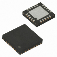
ATTINY43U-MU Atmel, ATTINY43U-MU Datasheet

ATTINY43U-MU
Specifications of ATTINY43U-MU
Related parts for ATTINY43U-MU
ATTINY43U-MU Summary of contents
Page 1
... Active Mode, 1 MHz System Clock (Without Boost Converter) 400 µ – Power-Down Mode (Without Boost Converter) 150 Note: 1. See “Data Retention” on page 6 ® 8-Bit Microcontroller (1) for details. 8-bit Microcontroller with 4K Bytes In-System Programmable Flash and Boost Converter ATtiny43U Preliminary Summary Rev. 8048BS–AVR–03/09 ...
Page 2
... Pin Configurations Figure 1-1. Pinout of ATtiny43U (T1/CLKO/PCINT11) PB (DI/OC1A/PCINT12) (DO/OC1B/PCINT13) (USCK/SCL/PCINT14) 1.1 Pin Descriptions 1.1 Supply voltage. 1.1.2 GND Ground. 1.1.3 Port A (PA7:PA0) Port 8-bit bi-directional I/O port with internal pull-up resistors (selected for each bit). The Port A output buffers have symmetrical drive characteristics with both high sink and source ...
Page 3
PA7 which has the RESET capability. To use pin PA7 as an I/O pin, instead of RESET pin, program (‘0’) RSTDISBL fuse. As inputs, Port A pins that are externally pulled low will source current if the pull-up ...
Page 4
... Overview The ATtiny43U is a low-power CMOS 8-bit microcontroller based on the AVR enhanced RISC architecture. By executing powerful instructions in a single clock cycle, the ATtiny43U achieves throughputs approaching 1 MIPS per MHz allowing the system designer to optimize power con- sumption versus processing speed. Figure 2-1. ...
Page 5
... On-chip ISP Flash allows the Program memory to be re-programmed In-System through an SPI serial interface conventional non-volatile memory programmer On-chip boot code running on the AVR core. The ATtiny43U AVR is supported by a full suite of program and system development tools including: C Compilers, Macro Assemblers, Program Debugger/Simulators, In-Circuit Emulators, and Evaluation kits. ...
Page 6
... PPM over 20 years at 85°C or 100 years at 25°C. 3.4 Disclaimer Typical values contained in this data sheet are based on simulations and characterization of other AVR microcontrollers manufactured on the same process technology. Min and Max val- ues will be available after the device is characterized. ATtiny43U 6 8048BS–AVR–03/09 ...
Page 7
Register Summary Address Name Bit 7 0x3F (0x5F) SREG I – 0x3E (0x5E) SPH 0x3D (0x5D) SPL SP7 0x3C (0x5C) OCR0B 0x3B (0x5B) GIMSK – 0x3A (0x5A) GIFR – 0x39 (0x59) TIMSK0 – 0x38 (0x58) TIFR0 – 0x37 (0x57) ...
Page 8
... Some of the Status Flags are cleared by writing a logical one to them. Note that, unlike most other AVRs, the CBI and SBI instructions will only operation the specified bit, and can therefore be used on registers containing such Status Flags. The CBI and SBI instructions work with registers 0x00 to 0x1F only. ATtiny43U 8 8048BS–AVR–03/09 ...
Page 9
Instruction Set Summary Mnemonics Operands ARITHMETIC AND LOGIC INSTRUCTIONS ADD Rd, Rr Add two Registers ADC Rd, Rr Add with Carry two Registers ADIW Rdl,K Add Immediate to Word SUB Rd, Rr Subtract two Registers SUBI Rd, K Subtract ...
Page 10
... Rd Pop Register from Stack MCU CONTROL INSTRUCTIONS NOP No Operation SLEEP Sleep WDR Watchdog Reset BREAK Break ATtiny43U 10 Description Rd(7)←C,Rd(n)← Rd(n+1),C←Rd(0) Rd(n) ← Rd(n+1), n=0..6 Rd(3..0)←Rd(7..4),Rd(7..4)←Rd(3..0) SREG(s) ← 1 SREG(s) ← ← Rr(b) Rd(b) ← ← ← ← ...
Page 11
... Body, Quad Flat No-Lead/Micro Lead Frame Package (QFN/MLF) 20S2 20-lead, 0.300" Wide Body, Plastic Gull Wing Small Outline Package (SOIC) 8048BS–AVR–03/09 (1) Ordering Code ATtiny43U-MU (3) ATtiny43U-SU “Characteristics of Boost Converter -20°C ... +85°C, unless other- for more information. Package Type ...
Page 12
... TOP VIEW D2 Pin #1 Notch (0. BOTTOM VIEW Reference JEDEC Standard MO-220, Fig. 1 (SAW Singulation) WGGD-5. Note: 2325 Orchard Parkway San Jose, CA 95131 R ATtiny43U TITLE 20M1, 20-pad 0.8 mm Body, Lead Pitch 0.50 mm, 2.6 mm Exposed Pad, Micro Lead Frame Package (MLF) SIDE VIEW A2 ...
Page 13
7.2 20S2 8048BS–AVR–03/09 13 ...
Page 14
... Errata The revision letter in this section refers to the revision of the ATtiny43U device. 8.1 ATtiny43U 8.1.1 Rev. C • Increased Probability of Boost Converter Entering Active Low Current Mode 1. Increased Probability of Boost Converter Entering Active Low Current Mode The boost converter may enter and stay in Active Low Current Mode at supply voltages and load currents higher than those specified ...
Page 15
Datasheet Revision History 9.1 Rev. 8048B-03/09 1. 9.2 Rev. 8048A-02/09 1. 8048BS–AVR–03/09 Updated Data retention bullet in “Features” on page Initial revision ...
Page 16
... Disclaimer: The information in this document is provided in connection with Atmel products. No license, express or implied, by estoppel or otherwise, to any intellectual property right is granted by this document or in connection with the sale of Atmel products. EXCEPT AS SET FORTH IN ATMEL’S TERMS AND CONDI- TIONS OF SALE LOCATED ON ATMEL’S WEB SITE, ATMEL ASSUMES NO LIABILITY WHATSOEVER AND DISCLAIMS ANY EXPRESS, IMPLIED OR STATUTORY WARRANTY RELATING TO ITS PRODUCTS INCLUDING, BUT NOT LIMITED TO, THE IMPLIED WARRANTY OF MERCHANTABILITY, FITNESS FOR A PARTICULAR PURPOSE, OR NON-INFRINGEMENT ...


