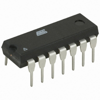
ATTINY84-20PU Atmel, ATTINY84-20PU Datasheet - Page 132

ATTINY84-20PU
Manufacturer Part Number
ATTINY84-20PU
Description
IC MCU AVR 8K FLASH 20MHZ 14-DIP
Manufacturer
Atmel
Series
AVR® ATtinyr
Specifications of ATTINY84-20PU
Core Processor
AVR
Core Size
8-Bit
Speed
20MHz
Connectivity
USI
Peripherals
Brown-out Detect/Reset, POR, PWM, Temp Sensor, WDT
Number Of I /o
12
Program Memory Size
8KB (4K x 16)
Program Memory Type
FLASH
Eeprom Size
512 x 8
Ram Size
512 x 8
Voltage - Supply (vcc/vdd)
2.7 V ~ 5.5 V
Data Converters
A/D 8x10b
Oscillator Type
Internal
Operating Temperature
-40°C ~ 85°C
Package / Case
14-DIP (0.300", 7.62mm)
Processor Series
ATTINY8x
Core
AVR8
Data Bus Width
8 bit
Data Ram Size
512 B
Interface Type
SPI
Maximum Clock Frequency
20 MHz
Number Of Programmable I/os
12
Number Of Timers
2
Operating Supply Voltage
2.7 V to 5.5 V
Maximum Operating Temperature
+ 85 C
Mounting Style
Through Hole
3rd Party Development Tools
EWAVR, EWAVR-BL
Development Tools By Supplier
ATAVRDRAGON, ATSTK500, ATSTK600, ATAVRISP2, ATAVRONEKIT
Minimum Operating Temperature
- 40 C
On-chip Adc
8-ch x 10-bit
Controller Family/series
AVR Tiny
No. Of I/o's
12
Eeprom Memory Size
512Byte
Ram Memory Size
512Byte
Cpu Speed
20MHz
No. Of Timers
2
Rohs Compliant
Yes
Package
14PDIP
Device Core
AVR
Family Name
ATtiny
Maximum Speed
20 MHz
For Use With
ATSTK600 - DEV KIT FOR AVR/AVR32770-1007 - ISP 4PORT ATMEL AVR MCU SPI/JTAGATAVRISP2 - PROGRAMMER AVR IN SYSTEM
Lead Free Status / RoHS Status
Lead free / RoHS Compliant
Available stocks
Company
Part Number
Manufacturer
Quantity
Price
Company:
Part Number:
ATTINY84-20PU
Manufacturer:
XILINX
Quantity:
25
- Current page: 132 of 238
- Download datasheet (5Mb)
16. Analog to Digital Converter
16.1
16.2
132
Features
Overview
ATtiny24/44/84
•
•
•
•
•
•
•
•
•
•
•
•
•
•
•
•
•
The ATtiny24/44/84 features a 10-bit successive approximation ADC. The ADC is connected to
8-pin port A for external sources. In addition to external sources internal temperature sensor can
be measured by ADC. Analog Multiplexer allows eight single-ended channels or 12 differential
channels from Port A. The programmable gain stage provides ampification steps 0 dB (1x) and
26 dB (20x) for 12 differential ADC channels.
The ADC contains a Sample and Hold circuit which ensures that the input voltage to the ADC is
held at a constant level during conversion. A block diagram of the ADC is shown in
on page
Internal reference voltage of nominally 1.1V is provided On-chip. Alternatively, V
as reference voltage for single ended channels. There is also an option to use an external volt-
age reference and turn-off the internal voltage reference.
10-bit Resolution
1.0 LSB Integral Non-linearity
± 2 LSB Absolute Accuracy
13µs Conversion Time
15 kSPS at Maximum Resolution
Eight Multiplexed Single Ended Input Channels
Twelve Differential Input Channels with Selectable Gain (1x, 20x)
Temperature Sensor Input Channel
Optional Left Adjustment for ADC Result Readout
0 - V
1.1V ADC Reference Voltage
Free Running or Single Conversion Mode
ADC Start Conversion by Auto Triggering on Interrupt Sources
Interrupt on ADC Conversion Complete
Sleep Mode Noise Canceler
Unipolar / Bipolar Input Mode
Input Polarity Reversal Mode
CC
133.
ADC Input Voltage Range
CC
8006K–AVR–10/10
can be used
Figure 16-1
Related parts for ATTINY84-20PU
Image
Part Number
Description
Manufacturer
Datasheet
Request
R

Part Number:
Description:
Manufacturer:
Atmel Corporation
Datasheet:

Part Number:
Description:
Manufacturer:
Atmel Corporation
Datasheet:

Part Number:
Description:
IC MCU AVR 8K FLASH 20MHZ 20-QFN
Manufacturer:
Atmel
Datasheet:

Part Number:
Description:
MCU AVR 8K ISP FLASH 2.7V 14SOIC
Manufacturer:
Atmel
Datasheet:

Part Number:
Description:
MCU AVR 8K FLASH 15MHZ 20-QFN
Manufacturer:
Atmel
Datasheet:

Part Number:
Description:
MCU AVR 8KB FLASH 10MHZ 14SOIC
Manufacturer:
Atmel
Datasheet:

Part Number:
Description:
MCU AVR 8KB FLASH 20MHZ 20QFN
Manufacturer:
Atmel
Datasheet:

Part Number:
Description:
DEV KIT FOR AVR/AVR32
Manufacturer:
Atmel
Datasheet:

Part Number:
Description:
INTERVAL AND WIPE/WASH WIPER CONTROL IC WITH DELAY
Manufacturer:
ATMEL Corporation
Datasheet:

Part Number:
Description:
Low-Voltage Voice-Switched IC for Hands-Free Operation
Manufacturer:
ATMEL Corporation
Datasheet:

Part Number:
Description:
MONOLITHIC INTEGRATED FEATUREPHONE CIRCUIT
Manufacturer:
ATMEL Corporation
Datasheet:

Part Number:
Description:
AM-FM Receiver IC U4255BM-M
Manufacturer:
ATMEL Corporation
Datasheet:

Part Number:
Description:
Monolithic Integrated Feature Phone Circuit
Manufacturer:
ATMEL Corporation
Datasheet:

Part Number:
Description:
Multistandard Video-IF and Quasi Parallel Sound Processing
Manufacturer:
ATMEL Corporation
Datasheet:


