ATTINY84-20PU Atmel, ATTINY84-20PU Datasheet - Page 69
ATTINY84-20PU
Manufacturer Part Number
ATTINY84-20PU
Description
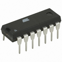
IC MCU AVR 8K FLASH 20MHZ 14-DIP
Manufacturer
Atmel
Series
AVR® ATtinyr
Specifications of ATTINY84-20PU
Core Processor
AVR
Core Size
8-Bit
Speed
20MHz
Connectivity
USI
Peripherals
Brown-out Detect/Reset, POR, PWM, Temp Sensor, WDT
Number Of I /o
12
Program Memory Size
8KB (4K x 16)
Program Memory Type
FLASH
Eeprom Size
512 x 8
Ram Size
512 x 8
Voltage - Supply (vcc/vdd)
2.7 V ~ 5.5 V
Data Converters
A/D 8x10b
Oscillator Type
Internal
Operating Temperature
-40°C ~ 85°C
Package / Case
14-DIP (0.300", 7.62mm)
Processor Series
ATTINY8x
Core
AVR8
Data Bus Width
8 bit
Data Ram Size
512 B
Interface Type
SPI
Maximum Clock Frequency
20 MHz
Number Of Programmable I/os
12
Number Of Timers
2
Operating Supply Voltage
2.7 V to 5.5 V
Maximum Operating Temperature
+ 85 C
Mounting Style
Through Hole
3rd Party Development Tools
EWAVR, EWAVR-BL
Development Tools By Supplier
ATAVRDRAGON, ATSTK500, ATSTK600, ATAVRISP2, ATAVRONEKIT
Minimum Operating Temperature
- 40 C
On-chip Adc
8-ch x 10-bit
Controller Family/series
AVR Tiny
No. Of I/o's
12
Eeprom Memory Size
512Byte
Ram Memory Size
512Byte
Cpu Speed
20MHz
No. Of Timers
2
Rohs Compliant
Yes
Package
14PDIP
Device Core
AVR
Family Name
ATtiny
Maximum Speed
20 MHz
For Use With
ATSTK600 - DEV KIT FOR AVR/AVR32770-1007 - ISP 4PORT ATMEL AVR MCU SPI/JTAGATAVRISP2 - PROGRAMMER AVR IN SYSTEM
Lead Free Status / RoHS Status
Lead free / RoHS Compliant
Available stocks
Company
Part Number
Manufacturer
Quantity
Price
Company:

Part Number:
ATTINY84-20PU
Manufacturer:
XILINX
Quantity:
25


11. 8-bit Timer/Counter0 with PWM
11.1
11.2
8006K–AVR–10/10
Features
Overview
•
•
•
•
•
•
•
Timer/Counter0 is a general purpose 8-bit Timer/Counter module, with two independent Output
Compare Units, and with PWM support. It allows accurate program execution timing (event man-
agement) and wave generation.
A simplified block diagram of the 8-bit Timer/Counter is shown in
the actual placement of I/O pins, refer to
including I/O bits and I/O pins, are shown in bold. The device-specific I/O Register and bit loca-
tions are listed in the
Figure 11-1. 8-bit Timer/Counter Block Diagram
Two Independent Output Compare Units
Double Buffered Output Compare Registers
Clear Timer on Compare Match (Auto Reload)
Glitch Free, Phase Correct Pulse Width Modulator (PWM)
Variable PWM Period
Frequency Generator
Three Independent Interrupt Sources (TOV0, OCF0A, and OCF0B)
Timer/Counter
TCCRnA
OCRnA
TCNTn
OCRnB
=
=
“Register Description” on page
Direction
Count
Clear
Control Logic
TOP
Figure 1-1 on page
=
TCCRnB
Value
BOTTOM
Fixed
TOP
clk
80.
=
Tn
0
2. CPU accessible I/O Registers,
OCnA
(Int.Req.)
OCnB
(Int.Req.)
Figure 11-1 on page
TOVn
(Int.Req.)
Clock Select
ATtiny24/44/84
Generation
Generation
( From Prescaler )
Waveform
Waveform
Detector
Edge
69. For
OCnA
OCnB
Tn
69
Related parts for ATTINY84-20PU
Image
Part Number
Description
Manufacturer
Datasheet
Request
R

Part Number:
Description:
Manufacturer:
Atmel Corporation
Datasheet:
Part Number:
Description:
Manufacturer:
Atmel Corporation
Datasheet:

Part Number:
Description:
IC MCU AVR 8K FLASH 20MHZ 20-QFN
Manufacturer:
Atmel
Datasheet:

Part Number:
Description:
MCU AVR 8K ISP FLASH 2.7V 14SOIC
Manufacturer:
Atmel
Datasheet:

Part Number:
Description:
MCU AVR 8K FLASH 15MHZ 20-QFN
Manufacturer:
Atmel
Datasheet:

Part Number:
Description:
MCU AVR 8KB FLASH 10MHZ 14SOIC
Manufacturer:
Atmel
Datasheet:
Part Number:
Description:
MCU AVR 8KB FLASH 20MHZ 20QFN
Manufacturer:
Atmel
Datasheet:

Part Number:
Description:
DEV KIT FOR AVR/AVR32
Manufacturer:
Atmel
Datasheet:
Part Number:
Description:
INTERVAL AND WIPE/WASH WIPER CONTROL IC WITH DELAY
Manufacturer:
ATMEL Corporation
Datasheet:
Part Number:
Description:
Low-Voltage Voice-Switched IC for Hands-Free Operation
Manufacturer:
ATMEL Corporation
Datasheet:
Part Number:
Description:
MONOLITHIC INTEGRATED FEATUREPHONE CIRCUIT
Manufacturer:
ATMEL Corporation
Datasheet:
Part Number:
Description:
AM-FM Receiver IC U4255BM-M
Manufacturer:
ATMEL Corporation
Datasheet:
Part Number:
Description:
Monolithic Integrated Feature Phone Circuit
Manufacturer:
ATMEL Corporation
Datasheet:
Part Number:
Description:
Multistandard Video-IF and Quasi Parallel Sound Processing
Manufacturer:
ATMEL Corporation
Datasheet: