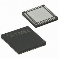
ATMEGA8515L-8MU Atmel, ATMEGA8515L-8MU Datasheet - Page 20

ATMEGA8515L-8MU
Manufacturer Part Number
ATMEGA8515L-8MU
Description
IC AVR MCU 8K 8MHZ 3V 44-QFN
Manufacturer
Atmel
Series
AVR® ATmegar
Specifications of ATMEGA8515L-8MU
Core Processor
AVR
Core Size
8-Bit
Speed
8MHz
Connectivity
EBI/EMI, SPI, UART/USART
Peripherals
Brown-out Detect/Reset, POR, PWM, WDT
Number Of I /o
35
Program Memory Size
8KB (4K x 16)
Program Memory Type
FLASH
Eeprom Size
512 x 8
Ram Size
512 x 8
Voltage - Supply (vcc/vdd)
2.7 V ~ 5.5 V
Oscillator Type
Internal
Operating Temperature
-40°C ~ 85°C
Package / Case
44-VQFN Exposed Pad
Processor Series
ATMEGA8x
Core
AVR8
Data Bus Width
8 bit
Data Ram Size
512 B
Interface Type
SPI, USART
Maximum Clock Frequency
8 MHz
Number Of Programmable I/os
35
Number Of Timers
2
Operating Supply Voltage
2.7 V to 5.5 V
Maximum Operating Temperature
+ 85 C
Mounting Style
SMD/SMT
3rd Party Development Tools
EWAVR, EWAVR-BL
Minimum Operating Temperature
- 40 C
For Use With
ATAVRISP2 - PROGRAMMER AVR IN SYSTEMATSTK500 - PROGRAMMER AVR STARTER KIT
Lead Free Status / RoHS Status
Lead free / RoHS Compliant
Data Converters
-
Lead Free Status / Rohs Status
Details
Available stocks
Company
Part Number
Manufacturer
Quantity
Price
Part Number:
ATMEGA8515L-8MU
Manufacturer:
ATMEL/爱特梅尔
Quantity:
20 000
- Current page: 20 of 257
- Download datasheet (2Mb)
The EEPROM Data Register –
EEDR
The EEPROM Control Register
– EECR
20
ATmega8515(L)
• Bits 7..0 – EEDR7.0: EEPROM Data
For the EEPROM write operation, the EEDR Register contains the data to be written to
the EEPROM in the address given by the EEAR Register. For the EEPROM read oper-
ation, the EEDR contains the data read out from the EEPROM at the address given by
EEAR.
• Bits 7..4 – Res: Reserved Bits
These bits are reserved bits in the ATmega8515 and will always read as zero.
• Bit 3 – EERIE: EEPROM Ready Interrupt Enable
Writing EERIE to one enables the EEPROM Ready Interrupt if the I-bit in SREG is set.
Writing EERIE to zero disables the interrupt. The EEPROM Ready interrupt generates a
constant interrupt when EEWE is cleared.
• Bit 2 – EEMWE: EEPROM Master Write Enable
The EEMWE bit determines whether setting EEWE to one causes the EEPROM to be
written. When EEMWE is set, setting EEWE within four clock cycles will write data to the
EEPROM at the selected address If EEMWE is zero, setting EEWE will have no effect.
When EEMWE has been written to one by software, hardware clears the bit to zero after
four clock cycles. See the description of the EEWE bit for an EEPROM write procedure.
• Bit 1 – EEWE: EEPROM Write Enable
The EEPROM Write Enable Signal EEWE is the write strobe to the EEPROM. When
address and data are correctly set up, the EEWE bit must be written to one to write the
value into the EEPROM. The EEMWE bit must be written to one before a logical one is
written to EEWE, otherwise no EEPROM write takes place. The following procedure
should be followed when writing the EEPROM (the order of steps 3 and 4 is not
essential):
1. Wait until EEWE becomes zero.
2. Wait until SPMEN in SPMCR becomes zero.
3. Write new EEPROM address to EEAR (optional).
4. Write new EEPROM data to EEDR (optional).
5. Write a logical one to the EEMWE bit while writing a zero to EEWE in EECR.
6. Within four clock cycles after setting EEMWE, write a logical one to EEWE.
The EEPROM can not be programmed during a CPU write to the Flash memory. The
software must check that the Flash programming is completed before initiating a new
EEPROM write. Step 2 is only relevant if the software contains a Boot Loader allowing
the CPU to program the Flash. If the Flash is never being updated by the CPU, step 2
can be omitted. See “Boot Loader Support – Read-While-Write Self-Programming” on
page 166 for details about boot programming.
Bit
Read/Write
Initial Value
Bit
Read/Write
Initial Value
MSB
R/W
R
7
0
7
–
0
R/W
R
6
0
6
–
0
R/W
R
5
0
5
–
0
R/W
R
4
0
4
–
0
EERIE
R/W
R/W
3
0
3
0
EEMWE
R/W
R/W
2
0
2
0
EEWE
R/W
R/W
1
0
X
1
EERE
LSB
R/W
R/W
0
0
0
0
2512K–AVR–01/10
EEDR
EECR
Related parts for ATMEGA8515L-8MU
Image
Part Number
Description
Manufacturer
Datasheet
Request
R

Part Number:
Description:
IC AVR MCU 2.4GHZ XCEIVER 64QFN
Manufacturer:
Atmel
Datasheet:

Part Number:
Description:
Manufacturer:
Atmel
Datasheet:

Part Number:
Description:
MCU ATMEGA644/AT86RF230 40-DIP
Manufacturer:
Atmel
Datasheet:

Part Number:
Description:
BUNDLE ATMEGA644P/AT86RF230 QFN
Manufacturer:
Atmel
Datasheet:

Part Number:
Description:
BUNDLE ATMEGA644P/AT86RF230 TQFP
Manufacturer:
Atmel
Datasheet:

Part Number:
Description:
MCU ATMEGA1281/AT86RF230 64-TQFP
Manufacturer:
Atmel
Datasheet:

Part Number:
Description:
MCU ATMEGA1280/AT86RF230 100TQFP
Manufacturer:
Atmel
Datasheet:

Part Number:
Description:
BUNDLE ATMEGA1280/AT86RF100-TQFP
Manufacturer:
Atmel
Datasheet:

Part Number:
Description:
BUNDLE ATMEGA2560V/AT86RF230-ZU
Manufacturer:
Atmel
Datasheet:

Part Number:
Description:
MCU ATMEGA2561/AT86RF230 64-TQFP
Manufacturer:
Atmel
Datasheet:

Part Number:
Description:
INTERVAL AND WIPE/WASH WIPER CONTROL IC WITH DELAY
Manufacturer:
ATMEL Corporation
Datasheet:

Part Number:
Description:
Low-Voltage Voice-Switched IC for Hands-Free Operation
Manufacturer:
ATMEL Corporation
Datasheet:

Part Number:
Description:
MONOLITHIC INTEGRATED FEATUREPHONE CIRCUIT
Manufacturer:
ATMEL Corporation
Datasheet:

Part Number:
Description:
AM-FM Receiver IC U4255BM-M
Manufacturer:
ATMEL Corporation
Datasheet:


