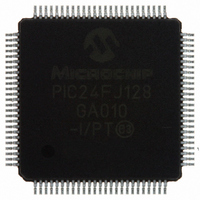
PIC24FJ128GA010-I/PT Microchip Technology, PIC24FJ128GA010-I/PT Datasheet - Page 18

PIC24FJ128GA010-I/PT
Manufacturer Part Number
PIC24FJ128GA010-I/PT
Description
IC PIC MCU FLASH 128K 100TQFP
Manufacturer
Microchip Technology
Series
PIC® 24Fr
Datasheets
1.PIC24FJ16GA002-ISS.pdf
(52 pages)
2.PIC24FJ64GA006-IPT.pdf
(240 pages)
3.PIC24FJ64GA006-IPT.pdf
(22 pages)
4.PIC24FJ128GA008-IPT.pdf
(12 pages)
5.PIC24FJ128GA006-IPT.pdf
(231 pages)
6.PIC24FJ128GA010-IPT.pdf
(230 pages)
Specifications of PIC24FJ128GA010-I/PT
Core Size
16-Bit
Program Memory Size
128KB (43K x 24)
Core Processor
PIC
Speed
16MHz
Connectivity
I²C, PMP, SPI, UART/USART
Peripherals
Brown-out Detect/Reset, POR, PWM, WDT
Number Of I /o
84
Program Memory Type
FLASH
Ram Size
8K x 8
Voltage - Supply (vcc/vdd)
2 V ~ 3.6 V
Data Converters
A/D 16x10b
Oscillator Type
Internal
Operating Temperature
-40°C ~ 85°C
Package / Case
100-TFQFP
Controller Family/series
PIC24
No. Of I/o's
84
Ram Memory Size
8KB
Cpu Speed
32MHz
No. Of Timers
5
No. Of Pwm Channels
5
Embedded Interface Type
EUART, I2C, PSP, SPI
Rohs Compliant
Yes
Processor Series
PIC24FJ
Core
PIC
Data Bus Width
16 bit
Data Ram Size
8 KB
Interface Type
SPI, I2C, USART
Maximum Clock Frequency
16 MHz
Number Of Programmable I/os
54
Number Of Timers
5
Maximum Operating Temperature
+ 85 C
Mounting Style
SMD/SMT
3rd Party Development Tools
52713-733, 52714-737, 53276-922, EWDSPIC
Development Tools By Supplier
PG164130, DV164035, DV244005, DV164005, PG164120, DM240001, DM240011
Minimum Operating Temperature
- 40 C
On-chip Adc
10 bit, 16 Channel
Package
100TQFP
Device Core
PIC
Family Name
PIC24
Maximum Speed
16 MHz
Operating Supply Voltage
2.5|3.3 V
Lead Free Status / RoHS Status
Lead free / RoHS Compliant
For Use With
DM240011 - KIT STARTER MPLAB FOR PIC24F MCUAC164333 - MODULE SKT FOR PM3 100QFPDV164033 - KIT START EXPLORER 16 MPLAB ICD2MA160011 - DAUGHTER BOARD PICDEM LCD 16F91XDM240001 - BOARD DEMO PIC24/DSPIC33/PIC32
Eeprom Size
-
Lead Free Status / Rohs Status
Details
Available stocks
Company
Part Number
Manufacturer
Quantity
Price
Company:
Part Number:
PIC24FJ128GA010-I/PT
Manufacturer:
Microchi
Quantity:
627
Company:
Part Number:
PIC24FJ128GA010-I/PT
Manufacturer:
MICROCHIP
Quantity:
212
Company:
Part Number:
PIC24FJ128GA010-I/PT
Manufacturer:
Microchip Technology
Quantity:
10 000
PIC24FJXXXGA0XX
3.6
The procedure for writing code memory is the same as
the procedure for writing the Configuration registers,
except that 64 instruction words are programmed at a
time. To facilitate this operation, working registers,
W0:W5, are used as temporary holding registers for the
data to be programmed.
Table 3-5 shows the ICSP programming details, includ-
ing the serial pattern with the ICSP command code
which must be transmitted, Least Significant bit first,
using the PGCx and PGDx pins (see Figure 3-2).
In Step 1, the Reset vector is exited. In Step 2, the
NVMCON register is initialized for programming a full
row of code memory. In Step 3, the 24-bit starting des-
tination address for programming is loaded into the
TBLPAG register and W7 register. (The upper byte of
the starting destination address is stored in TBLPAG
and the lower 16 bits of the destination address are
stored in W7.)
To minimize the programming time, A packed instruction
format is used (Figure 3-6).
In Step 4, four packed instruction words are stored in
working registers, W0:W5, using the MOV instruction,
and the Read Pointer, W6, is initialized. The contents of
W0:W5 (holding the packed instruction word data) are
shown in Figure 3-6.
TABLE 3-5:
DS39768D-page 18
Command
Step 1: Exit the Reset vector.
Step 2: Set the NVMCON to program 64 instruction words.
Step 3: Initialize the Write Pointer (W7) for TBLWT instruction.
Step 4: Load W0:W5 with the next 4 instruction words to program.
(Binary)
0000
0000
0000
0000
0000
0000
0000
0000
0000
0000
0000
0000
0000
0000
Writing Code Memory
SERIAL INSTRUCTION EXECUTION FOR WRITING CODE MEMORY
000000
040200
000000
24001A
883B0A
200xx0
880190
2xxxx7
2xxxx0
2xxxx1
2xxxx2
2xxxx3
2xxxx4
2xxxx5
(Hex)
Data
NOP
GOTO
NOP
MOV
MOV
MOV
MOV
MOV
MOV
MOV
MOV
MOV
MOV
MOV
0x200
#0x4001, W10
W10, NVMCON
#<DestinationAddress23:16>, W0
W0, TBLPAG
#<DestinationAddress15:0>, W7
#<LSW0>, W0
#<MSB1:MSB0>, W1
#<LSW1>, W2
#<LSW2>, W3
#<MSB3:MSB2>, W4
#<LSW3>, W5
In Step 5, eight TBLWT instructions are used to copy
the data from W0:W5 to the write latches of code mem-
ory. Since code memory is programmed 64 instruction
words at a time, Steps 4 and 5 are repeated 16 times to
load all the write latches (Step 6).
After the write latches are loaded, programming is
initiated by writing to the NVMCON register in Steps 7
and 8. In Step 9, the internal PC is reset to 200h. This
is a precautionary measure to prevent the PC from
incrementing into unimplemented memory when large
devices are being programmed. Lastly, in Step 10,
Steps 3-9 are repeated until all of code memory is
programmed.
FIGURE 3-6:
W0
W1
W2
W3
W4
W5
Description
15
MSB1
MSB3
PACKED INSTRUCTION
WORDS IN W<0:5>
© 2008 Microchip Technology Inc.
LSW0
LSW1
LSW2
LSW3
8 7
MSB0
MSB2
0


