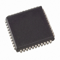
AT89C51ED2-SLSUM Atmel, AT89C51ED2-SLSUM Datasheet - Page 64

AT89C51ED2-SLSUM
Manufacturer Part Number
AT89C51ED2-SLSUM
Description
IC 8051 MCU FLASH 64K 44PLCC
Manufacturer
Atmel
Series
89Cr
Datasheet
1.ATWEBDVK-02RC.pdf
(137 pages)
Specifications of AT89C51ED2-SLSUM
Core Processor
8051
Core Size
8-Bit
Speed
60MHz
Connectivity
SPI, UART/USART
Peripherals
POR, PWM, WDT
Number Of I /o
34
Program Memory Size
64KB (64K x 8)
Program Memory Type
FLASH
Eeprom Size
2K x 8
Ram Size
2K x 8
Voltage - Supply (vcc/vdd)
2.7 V ~ 5.5 V
Oscillator Type
External
Operating Temperature
-40°C ~ 85°C
Package / Case
44-PLCC
Package
44PLCC
Device Core
8051
Family Name
89C
Maximum Speed
40 MHz
Operating Supply Voltage
3.3|5 V
Data Bus Width
8 Bit
Number Of Programmable I/os
34
Interface Type
SPI/UART
Number Of Timers
3
Processor Series
AT89x
Core
8051
Data Ram Size
2 KB
Maximum Clock Frequency
40 MHz
Maximum Operating Temperature
+ 85 C
Mounting Style
SMD/SMT
3rd Party Development Tools
PK51, CA51, A51, ULINK2
Minimum Operating Temperature
- 40 C
Cpu Family
AT89
Device Core Size
8b
Frequency (max)
40MHz
Total Internal Ram Size
2KB
# I/os (max)
34
Number Of Timers - General Purpose
3
Operating Supply Voltage (typ)
3.3/5V
Operating Supply Voltage (max)
5.5V
Operating Supply Voltage (min)
2.7V
Instruction Set Architecture
CISC
Operating Temp Range
-40C to 85C
Operating Temperature Classification
Industrial
Mounting
Surface Mount
Pin Count
44
Package Type
PLCC
For Use With
AT89OCD-01 - USB EMULATOR FOR AT8XC51 MCU
Lead Free Status / RoHS Status
Lead free / RoHS Compliant
Data Converters
-
Lead Free Status / Rohs Status
Lead free / RoHS Compliant
Available stocks
Company
Part Number
Manufacturer
Quantity
Price
Company:
Part Number:
AT89C51ED2-SLSUM
Manufacturer:
MITSUBISHI
Quantity:
43
Part Number:
AT89C51ED2-SLSUM
Manufacturer:
MICROCHIP/微芯
Quantity:
20 000
16.2.3
16.2.4
16.2.5
64
AT89C51RD2/ED2
SPI Serial Clock (SCK)
Slave Select (SS)
Baud Rate
This signal is used to synchronize the data movement both in and out of the devices through
their MOSI and MISO lines. It is driven by the Master for eight clock cycles which allows to
exchange one Byte on the serial lines.
Each Slave peripheral is selected by one Slave Select pin (SS). This signal must stay low for any
message for a Slave. It is obvious that only one Master (SS high level) can drive the network.
The Master may select each Slave device by software through port pins
vent bus conflicts on the MISO line, only one slave should be selected at a time by the Master
for a transmission.
In a Master configuration, the SS line can be used in conjunction with the MODF flag in the SPI
Status register (SPSTA) to prevent multiple masters from driving MOSI and SCK (see Error
conditions).
A high level on the SS pin puts the MISO line of a Slave SPI in a high-impedance state.
The SS pin could be used as a general-purpose if the following conditions are met:
Note:
In Master mode, the baud rate can be selected from a baud rate generator which is controlled by
three bits in the SPCON register: SPR2, SPR1 and SPR0.The Master clock is selected from one
of seven clock rates resulting from the division of the internal clock by 2, 4, 8, 16, 32, 64 or 128.
Table 16-1
Table 16-1.
• The device is configured as a Master and the SSDIS control bit in SPCON is set. This kind of
• The Device is configured as a Slave with CPHA and SSDIS control bits set
SPR2
configuration can be found when only one Master is driving the network and there is no way
that the SS pin could be pulled low. Therefore, the MODF flag in the SPSTA will never be
set
configuration can happen when the system comprises one Master and one Slave only.
Therefore, the device should always be selected and there is no reason that the Master uses
the SS pin to select the communicating Slave device.
0
0
0
0
1
1
1
1
(1)
.
1. Clearing SSDIS control bit does not clear MODF.
2. Special care should be taken not to set SSDIS control bit when CPHA = ’0’ because in this
mode, the SS is used to start the transmission.
gives the different clock rates selected by SPR2:SPR1:SPR0.
SPR1
SPI Master Baud Rate Selection
0
0
1
1
0
0
1
1
SPR0
0
1
0
1
0
1
0
1
F
F
F
F
F
F
CLK PERIPH
F
CLK PERIPH
CLK PERIPH
CLK PERIPH
Clock Rate
CLK PERIPH
CLK PERIPH
CLK PERIPH
Don’t Use
/128
/16
/32
/64
/8
/2
/4
Baud Rate Divisor (BD)
(Figure
No BRG
(2)
128
16
32
64
. This kind of
2
4
8
16-2). To pre-
4235K–8051–05/08


