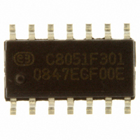
C8051F301-GS Silicon Laboratories Inc, C8051F301-GS Datasheet - Page 36

C8051F301-GS
Manufacturer Part Number
C8051F301-GS
Description
IC 8051 MCU 8K FLASH 14-SOIC
Manufacturer
Silicon Laboratories Inc
Series
C8051F30xr
Specifications of C8051F301-GS
Program Memory Type
FLASH
Program Memory Size
8KB (8K x 8)
Package / Case
14-SOIC (3.9mm Width), 14-SOL
Core Processor
8051
Core Size
8-Bit
Speed
25MHz
Connectivity
SMBus (2-Wire/I²C), UART/USART
Peripherals
POR, PWM, WDT
Number Of I /o
8
Ram Size
256 x 8
Voltage - Supply (vcc/vdd)
2.7 V ~ 3.6 V
Oscillator Type
Internal
Operating Temperature
-40°C ~ 85°C
Processor Series
C8051F3x
Core
8051
Data Bus Width
8 bit
Data Ram Size
256 B
Interface Type
I2C/SMBus/UART
Maximum Clock Frequency
25 MHz
Number Of Programmable I/os
8
Number Of Timers
3
Maximum Operating Temperature
+ 85 C
Mounting Style
SMD/SMT
3rd Party Development Tools
PK51, CA51, A51, ULINK2
Development Tools By Supplier
C8051F300DK
Minimum Operating Temperature
- 40 C
Package
14SOIC
Device Core
8051
Family Name
C8051F30x
Maximum Speed
25 MHz
Operating Supply Voltage
3.3 V
Lead Free Status / RoHS Status
Lead free / RoHS Compliant
For Use With
770-1006 - ISP 4PORT FOR SILABS C8051F MCU336-1444 - ADAPTER PROGRAM TOOLSTICK F300336-1319 - REFERENCE DESIGN STEPPER MOTOR
Eeprom Size
-
Data Converters
-
Lead Free Status / Rohs Status
Lead free / RoHS Compliant
Other names
336-1536-5
C8051F300/1/2/3/4/5
5.1.
The analog multiplexers (AMUX0) select the positive and negative inputs to the PGA, allowing any Port pin
to be measured relative to any other Port pin or GND. Additionally, the on-chip temperature sensor or the
positive power supply (V
negative input, ADC0 operates in Single-ended Mode; all other times, ADC0 operates in Differential
Mode. The ADC0 input channels are selected in the AMX0SL register as described in SFR Definition 5.1.
The conversion code format differs in Single-ended versus Differential modes, as shown below. When in
Single-ended Mode (negative input is selected GND), conversion codes are represented as 8-bit unsigned
integers. Inputs are measured from ‘0’ to VREF x 255/256. Example codes are shown below.
When in Differential Mode (negative input is not selected as GND), conversion codes are represented as
8-bit signed 2s complement numbers. Inputs are measured from –VREF to VREF x 127/128. Example
codes are shown below.
Important Note About ADC0 Input Configuration: Port pins selected as ADC0 inputs should be config-
ured as analog inputs and should be skipped by the Digital Crossbar. To configure a Port pin for analog
input, set to ‘0’ the corresponding bit in register P0MDIN. To force the Crossbar to skip a Port pin, set to ‘1’
the corresponding bit in register XBR0. See
I/O configuration details.
The PGA amplifies the AMUX0 output signal as defined by the AMP0GN1-0 bits in the ADC0 Configuration
register (SFR Definition 5.2). The PGA is software-programmable for gains of 0.5, 1, 2, or 4. The gain
defaults to 0.5 on reset.
5.2.
The typical temperature sensor transfer function is shown in Figure 5.2. The output voltage (V
positive PGA input when the temperature sensor is selected by bits AMX0P2-0 in register AMX0SL; this
voltage will be amplified by the PGA according to the user-programmed PGA settings.
36
Analog Multiplexer and PGA
Temperature Sensor
VREF x 127/128
–VREF x 64/128
VREF x 255/256
VREF x 128/256
VREF x 64/128
VREF x 64/256
Input Voltage
Input Voltage
DD
–VREF
) may be selected as the positive PGA input. When GND is selected as the
0
0
Section “12. Port Input/Output” on page 103
ADC0 Output (Conversion Code)
ADC0 Output (Conversion Code)
Rev. 2.9
0xFF
0xC0
0x80
0x40
0x00
0x7F
0x40
0x00
0x80
for more Port
TEMP
) is the


