C8051F314-GQ Silicon Laboratories Inc, C8051F314-GQ Datasheet - Page 132
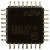
C8051F314-GQ
Manufacturer Part Number
C8051F314-GQ
Description
IC 8051 MCU 8K FLASH 32LQFP
Manufacturer
Silicon Laboratories Inc
Series
C8051F31xr
Specifications of C8051F314-GQ
Program Memory Type
FLASH
Program Memory Size
8KB (8K x 8)
Package / Case
32-LQFP
Core Processor
8051
Core Size
8-Bit
Speed
25MHz
Connectivity
SMBus (2-Wire/I²C), SPI, UART/USART
Peripherals
POR, PWM, WDT
Number Of I /o
29
Ram Size
1.25K x 8
Voltage - Supply (vcc/vdd)
2.7 V ~ 3.6 V
Oscillator Type
Internal
Operating Temperature
-40°C ~ 85°C
Processor Series
C8051F3x
Core
8051
Data Bus Width
8 bit
Data Ram Size
1.25 KB
Interface Type
I2C/SMBus/SPI/UART
Maximum Clock Frequency
25 MHz
Number Of Programmable I/os
29
Number Of Timers
4
Operating Supply Voltage
2.7 V to 3.6 V
Maximum Operating Temperature
+ 85 C
Mounting Style
SMD/SMT
3rd Party Development Tools
PK51, CA51, A51, ULINK2
Development Tools By Supplier
C8051F310DK
Minimum Operating Temperature
- 40 C
On-chip Adc
17-chx10-bit
No. Of I/o's
29
Ram Memory Size
1280Byte
Cpu Speed
25MHz
No. Of Timers
4
Rohs Compliant
Yes
Lead Free Status / RoHS Status
Lead free / RoHS Compliant
For Use With
770-1006 - ISP 4PORT FOR SILABS C8051F MCU336-1445 - ADAPTER PROGRAM TOOLSTICK F310
Eeprom Size
-
Data Converters
-
Lead Free Status / Rohs Status
Lead free / RoHS Compliant
Other names
336-1257
Available stocks
Company
Part Number
Manufacturer
Quantity
Price
Company:

Part Number:
C8051F314-GQ
Manufacturer:
Silicon Laboratories Inc
Quantity:
10 000
Company:
Part Number:
C8051F314-GQR
Manufacturer:
ST
Quantity:
15 000
Company:
Part Number:
C8051F314-GQR
Manufacturer:
Silicon Laboratories Inc
Quantity:
10 000


C8051F310/1/2/3/4/5/6/7
Registers XBR0 and XBR1 are used to assign the digital I/O resources to the physical I/O Port pins. Note
that when the SMBus is selected, the Crossbar assigns both pins associated with the SMBus (SDA and
SCL); when the UART is selected, the Crossbar assigns both pins associated with the UART (TX and RX).
UART0 pin assignments are fixed for bootloading purposes: UART TX0 is always assigned to P0.4; UART
RX0 is always assigned to P0.5. Standard Port I/Os appear contiguously after the prioritized functions
have been assigned.
Important Note: The SPI can be operated in either 3-wire or 4-wire modes, pending the state of the
NSSMD1-NSSMD0 bits in register SPI0CN. According to the SPI mode, the NSS signal may or may not be
routed to a Port pin.
132
*Note: NSS is only pinned out in 4-wire SPI mode.
SF Signals
PIN I/O
TX0
RX0
SCK
MISO
MOSI
NSS*
SDA
SCL
CP0
CP0A
CP1
CP1A
SYSCLK
CEX0
CEX1
CEX2
CEX3
CEX4
ECI
T0
T1
SF Signals
Note: P1.6,P1.7,P2.6,P2.7 only available on the C8051F310/1/2/3/4/5; P1SKIP[7:6] should always be set to
Figure 13.4. Crossbar Priority Decoder with Crystal Pins Skipped
11b for the C8051F316/7 devices.
Port pin potentially available to peripheral
Special Function Signals are not assigned by the Crossbar. When these signals are enabled, the Crossbar must
be manually configured to skip their corresponding port pins.
0
0
1
0
2
1
P0SKIP[0:7]
3
1
P0
4
0
5
0
6
0
7
0
0
0
Rev. 1.7
1
0
2
0
P1SKIP[0:7]
3
0
P1
4
0
5
0
6
0
7
0
0
0
P2SKIP[0:3]
1
0
2
0
3
0
P2
4
5
6
7
Related parts for C8051F314-GQ
Image
Part Number
Description
Manufacturer
Datasheet
Request
R

Part Number:
Description:
SMD/C°/SINGLE-ENDED OUTPUT SILICON OSCILLATOR
Manufacturer:
Silicon Laboratories Inc
Part Number:
Description:
Manufacturer:
Silicon Laboratories Inc
Datasheet:
Part Number:
Description:
N/A N/A/SI4010 AES KEYFOB DEMO WITH LCD RX
Manufacturer:
Silicon Laboratories Inc
Datasheet:
Part Number:
Description:
N/A N/A/SI4010 SIMPLIFIED KEY FOB DEMO WITH LED RX
Manufacturer:
Silicon Laboratories Inc
Datasheet:
Part Number:
Description:
N/A/-40 TO 85 OC/EZLINK MODULE; F930/4432 HIGH BAND (REV E/B1)
Manufacturer:
Silicon Laboratories Inc
Part Number:
Description:
EZLink Module; F930/4432 Low Band (rev e/B1)
Manufacturer:
Silicon Laboratories Inc
Part Number:
Description:
I°/4460 10 DBM RADIO TEST CARD 434 MHZ
Manufacturer:
Silicon Laboratories Inc
Part Number:
Description:
I°/4461 14 DBM RADIO TEST CARD 868 MHZ
Manufacturer:
Silicon Laboratories Inc
Part Number:
Description:
I°/4463 20 DBM RFSWITCH RADIO TEST CARD 460 MHZ
Manufacturer:
Silicon Laboratories Inc
Part Number:
Description:
I°/4463 20 DBM RADIO TEST CARD 868 MHZ
Manufacturer:
Silicon Laboratories Inc
Part Number:
Description:
I°/4463 27 DBM RADIO TEST CARD 868 MHZ
Manufacturer:
Silicon Laboratories Inc
Part Number:
Description:
I°/4463 SKYWORKS 30 DBM RADIO TEST CARD 915 MHZ
Manufacturer:
Silicon Laboratories Inc
Part Number:
Description:
N/A N/A/-40 TO 85 OC/4463 RFMD 30 DBM RADIO TEST CARD 915 MHZ
Manufacturer:
Silicon Laboratories Inc
Part Number:
Description:
I°/4463 20 DBM RADIO TEST CARD 169 MHZ
Manufacturer:
Silicon Laboratories Inc