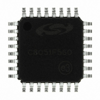
C8051F560-IQ Silicon Laboratories Inc, C8051F560-IQ Datasheet - Page 147

C8051F560-IQ
Manufacturer Part Number
C8051F560-IQ
Description
IC 8051 MCU 32K FLASH 32-QFP
Manufacturer
Silicon Laboratories Inc
Series
C8051F56xr
Specifications of C8051F560-IQ
Program Memory Type
FLASH
Program Memory Size
32KB (32K x 8)
Package / Case
32-QFP
Core Processor
8051
Core Size
8-Bit
Speed
50MHz
Connectivity
SMBus (2-Wire/I²C), CAN, LIN, SPI, UART/USART
Peripherals
POR, PWM, Temp Sensor, WDT
Number Of I /o
25
Ram Size
2.25K x 8
Voltage - Supply (vcc/vdd)
1.8 V ~ 5.25 V
Data Converters
A/D 25x12b
Oscillator Type
Internal
Operating Temperature
-40°C ~ 125°C
Processor Series
C8051F5x
Core
8051
Data Bus Width
8 bit
Data Ram Size
2304 B
Maximum Clock Frequency
50 MHz
Number Of Programmable I/os
25
Operating Supply Voltage
1.8 V to 5.25 V
Maximum Operating Temperature
+ 125 C
Mounting Style
SMD/SMT
3rd Party Development Tools
PK51, CA51, A51, ULINK2
Development Tools By Supplier
C8051F560DK
Minimum Operating Temperature
- 40 C
Lead Free Status / RoHS Status
Lead free / RoHS Compliant
For Use With
336-1691 - KIT DEVELOPMENT FOR C8051F560
Eeprom Size
-
Lead Free Status / Rohs Status
Lead free / RoHS Compliant
Other names
336-1693
Available stocks
Company
Part Number
Manufacturer
Quantity
Price
Company:
Part Number:
C8051F560-IQ
Manufacturer:
Silicon Laboratories Inc
Quantity:
10 000
Company:
Part Number:
C8051F560-IQR
Manufacturer:
Silicon Laboratories Inc
Quantity:
10 000
- Current page: 147 of 302
- Download datasheet (3Mb)
17.4. Multiplexed Mode
The External Memory Interface operates only in a Multiplexed mode. In Multiplexed mode, the Data Bus
and the lower 8-bits of the Address Bus share the same Port pins: AD[7:0]. In this mode, an external latch
(74HC373 or equivalent logic gate) is used to hold the lower 8-bits of the RAM address. The external latch
is controlled by the ALE (Address Latch Enable) signal, which is driven by the External Memory Interface
logic. An example of a Multiplexed Configuration is shown in Figure 17.1.
In Multiplexed mode, the external MOVX operation can be broken into two phases delineated by the state
of the ALE signal. During the first phase, ALE is high and the lower 8-bits of the Address Bus are pre-
sented to AD[7:0]. During this phase, the address latch is configured such that the Q outputs reflect the
states of the ‘D’ inputs. When ALE falls, signaling the beginning of the second phase, the address latch
outputs remain fixed and are no longer dependent on the latch inputs. Later in the second phase, the Data
Bus controls the state of the AD[7:0] port at the time RD or WR is asserted.
See Section “17.6.1. Multiplexed Mode” on page 151 for more information.
E
M
I
F
AD[7:0]
A[15:8]
/WR
ALE
/RD
Figure 17.1. Multiplexed Configuration Example
ADDRESS/DATA BUS
ADDRESS BUS
Rev. 1.1
V
DD
8
(Optional)
74HC373
G
D
C8051F55x/56x/57x
Q
A[15:8]
A[7:0]
I/O[7:0]
CE
WE
OE
64 K X 8
SRAM
147
Related parts for C8051F560-IQ
Image
Part Number
Description
Manufacturer
Datasheet
Request
R
Part Number:
Description:
SMD/C°/SINGLE-ENDED OUTPUT SILICON OSCILLATOR
Manufacturer:
Silicon Laboratories Inc
Part Number:
Description:
Manufacturer:
Silicon Laboratories Inc
Datasheet:
Part Number:
Description:
N/A N/A/SI4010 AES KEYFOB DEMO WITH LCD RX
Manufacturer:
Silicon Laboratories Inc
Datasheet:
Part Number:
Description:
N/A N/A/SI4010 SIMPLIFIED KEY FOB DEMO WITH LED RX
Manufacturer:
Silicon Laboratories Inc
Datasheet:
Part Number:
Description:
N/A/-40 TO 85 OC/EZLINK MODULE; F930/4432 HIGH BAND (REV E/B1)
Manufacturer:
Silicon Laboratories Inc
Part Number:
Description:
EZLink Module; F930/4432 Low Band (rev e/B1)
Manufacturer:
Silicon Laboratories Inc
Part Number:
Description:
I°/4460 10 DBM RADIO TEST CARD 434 MHZ
Manufacturer:
Silicon Laboratories Inc
Part Number:
Description:
I°/4461 14 DBM RADIO TEST CARD 868 MHZ
Manufacturer:
Silicon Laboratories Inc
Part Number:
Description:
I°/4463 20 DBM RFSWITCH RADIO TEST CARD 460 MHZ
Manufacturer:
Silicon Laboratories Inc
Part Number:
Description:
I°/4463 20 DBM RADIO TEST CARD 868 MHZ
Manufacturer:
Silicon Laboratories Inc
Part Number:
Description:
I°/4463 27 DBM RADIO TEST CARD 868 MHZ
Manufacturer:
Silicon Laboratories Inc
Part Number:
Description:
I°/4463 SKYWORKS 30 DBM RADIO TEST CARD 915 MHZ
Manufacturer:
Silicon Laboratories Inc
Part Number:
Description:
N/A N/A/-40 TO 85 OC/4463 RFMD 30 DBM RADIO TEST CARD 915 MHZ
Manufacturer:
Silicon Laboratories Inc
Part Number:
Description:
I°/4463 20 DBM RADIO TEST CARD 169 MHZ
Manufacturer:
Silicon Laboratories Inc


