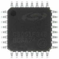
C8051F34B-GQ Silicon Laboratories Inc, C8051F34B-GQ Datasheet - Page 167

C8051F34B-GQ
Manufacturer Part Number
C8051F34B-GQ
Description
IC 8051 MCU 32K FLASH 32LQFP
Manufacturer
Silicon Laboratories Inc
Series
C8051F34xr
Datasheet
1.C8051F349-GQ.pdf
(276 pages)
Specifications of C8051F34B-GQ
Program Memory Type
FLASH
Program Memory Size
32KB (32K x 8)
Package / Case
32-LQFP
Core Processor
8051
Core Size
8-Bit
Speed
48MHz
Connectivity
SMBus (2-Wire/I²C), SPI, UART/USART, USB
Peripherals
Brown-out Detect/Reset, POR, PWM, Temp Sensor, WDT
Number Of I /o
25
Ram Size
2.25K x 8
Voltage - Supply (vcc/vdd)
2.7 V ~ 3.6 V
Data Converters
A/D 17x10b
Oscillator Type
Internal
Operating Temperature
-40°C ~ 85°C
Processor Series
C8051F3x
Core
8051
Data Bus Width
8 bit
Data Ram Size
2.25 KB
Interface Type
I2C/SMBus/SPI/UART/USB
Maximum Clock Frequency
48 MHz
Number Of Programmable I/os
25
Number Of Timers
4
Maximum Operating Temperature
+ 85 C
Mounting Style
SMD/SMT
3rd Party Development Tools
KSK-SL-F34X, KSK-SL-TOOLSTICK, PK51, CA51, A51, ULINK2
Development Tools By Supplier
C8051F340DK
Minimum Operating Temperature
- 40 C
Package
32LQFP
Device Core
8051
Family Name
C8051F34x
Maximum Speed
48 MHz
Operating Supply Voltage
3.3|5 V
On-chip Adc
17-chx10-bit
Lead Free Status / RoHS Status
Lead free / RoHS Compliant
For Use With
336-1748 - ADAPTER TOOLSTICK FOR C8051F34X
Eeprom Size
-
Lead Free Status / Rohs Status
Lead free / RoHS Compliant
Other names
336-1534
Available stocks
Company
Part Number
Manufacturer
Quantity
Price
Company:
Part Number:
C8051F34B-GQ
Manufacturer:
Silicon Laboratories Inc
Quantity:
10 000
Company:
Part Number:
C8051F34B-GQR
Manufacturer:
Silicon Laboratories Inc
Quantity:
10 000
- Current page: 167 of 276
- Download datasheet (2Mb)
16.5. FIFO Management
1024 bytes of on-chip XRAM are used as FIFO space for USB0. This FIFO space is split between
Endpoints0-3 as shown in Figure 16.3. FIFO space allocated for Endpoints1-3 is configurable as IN, OUT,
or both (Split Mode: half IN, half OUT).
16.5.1. FIFO Split Mode
The FIFO space for Endpoints1-3 can be split such that the upper half of the FIFO space is used by the IN
endpoint, and the lower half is used by the OUT endpoint. For example: if the Endpoint3 FIFO is configured
for Split Mode, the upper 256 bytes (0x0540 to 0x063F) are used by Endpoint3 IN and the lower 256 bytes
(0x0440 to 0x053F) are used by Endpoint3 OUT.
If an endpoint FIFO is not configured for Split Mode, that endpoint IN/OUT pair’s FIFOs are combined to
form a single IN or OUT FIFO. In this case only one direction of the endpoint IN/OUT pair may be used at
a time. The endpoint direction (IN/OUT) is determined by the DIRSEL bit in the corresponding endpoint’s
EINCSRH register (see SFR Definition 16.20).
0x07FF
0x07C0
0x07BF
0x03FF
0x073F
0x063F
0x043F
0x0740
0x0640
0x0440
0x0400
0x0000
C8051F340/1/2/3/4/5/6/7/8/9/A/B/C/D
Figure 16.3. USB FIFO Allocation
(1024 bytes)
User XRAM
(128 bytes)
(256 bytes)
(512 bytes)
Endpoint0
Endpoint1
Endpoint2
Endpoint3
(64 bytes)
(64 bytes)
Free
Rev. 1.3
USB Clock Domain
System Clock Domain
IN, OUT, or both (Split
Configurable as
Mode)
167
Related parts for C8051F34B-GQ
Image
Part Number
Description
Manufacturer
Datasheet
Request
R
Part Number:
Description:
SMD/C°/SINGLE-ENDED OUTPUT SILICON OSCILLATOR
Manufacturer:
Silicon Laboratories Inc
Part Number:
Description:
Manufacturer:
Silicon Laboratories Inc
Datasheet:
Part Number:
Description:
N/A N/A/SI4010 AES KEYFOB DEMO WITH LCD RX
Manufacturer:
Silicon Laboratories Inc
Datasheet:
Part Number:
Description:
N/A N/A/SI4010 SIMPLIFIED KEY FOB DEMO WITH LED RX
Manufacturer:
Silicon Laboratories Inc
Datasheet:
Part Number:
Description:
N/A/-40 TO 85 OC/EZLINK MODULE; F930/4432 HIGH BAND (REV E/B1)
Manufacturer:
Silicon Laboratories Inc
Part Number:
Description:
EZLink Module; F930/4432 Low Band (rev e/B1)
Manufacturer:
Silicon Laboratories Inc
Part Number:
Description:
I°/4460 10 DBM RADIO TEST CARD 434 MHZ
Manufacturer:
Silicon Laboratories Inc
Part Number:
Description:
I°/4461 14 DBM RADIO TEST CARD 868 MHZ
Manufacturer:
Silicon Laboratories Inc
Part Number:
Description:
I°/4463 20 DBM RFSWITCH RADIO TEST CARD 460 MHZ
Manufacturer:
Silicon Laboratories Inc
Part Number:
Description:
I°/4463 20 DBM RADIO TEST CARD 868 MHZ
Manufacturer:
Silicon Laboratories Inc
Part Number:
Description:
I°/4463 27 DBM RADIO TEST CARD 868 MHZ
Manufacturer:
Silicon Laboratories Inc
Part Number:
Description:
I°/4463 SKYWORKS 30 DBM RADIO TEST CARD 915 MHZ
Manufacturer:
Silicon Laboratories Inc
Part Number:
Description:
N/A N/A/-40 TO 85 OC/4463 RFMD 30 DBM RADIO TEST CARD 915 MHZ
Manufacturer:
Silicon Laboratories Inc
Part Number:
Description:
I°/4463 20 DBM RADIO TEST CARD 169 MHZ
Manufacturer:
Silicon Laboratories Inc


