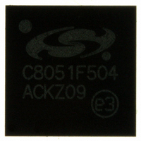
C8051F504-IM Silicon Laboratories Inc, C8051F504-IM Datasheet - Page 137

C8051F504-IM
Manufacturer Part Number
C8051F504-IM
Description
IC 8051 MCU 32K FLASH 48-QFN
Manufacturer
Silicon Laboratories Inc
Series
C8051F50xr
Specifications of C8051F504-IM
Program Memory Type
FLASH
Program Memory Size
32KB (32K x 8)
Package / Case
48-QFN
Mfg Application Notes
LIN Bootloader AppNote
Core Processor
8051
Core Size
8-Bit
Speed
50MHz
Connectivity
EBI/EMI, SMBus (2-Wire/I²C), CAN, LIN, SPI, UART/USART
Peripherals
POR, PWM, Temp Sensor, WDT
Number Of I /o
40
Ram Size
4.25K x 8
Voltage - Supply (vcc/vdd)
1.8 V ~ 5.25 V
Data Converters
A/D 32x12b
Oscillator Type
Internal
Operating Temperature
-40°C ~ 125°C
Processor Series
C8051F5x
Core
8051
Data Bus Width
8 bit
Data Ram Size
4.25 KB
Interface Type
I2C/SPI/UART
Maximum Clock Frequency
50 MHz
Number Of Programmable I/os
40
Number Of Timers
4
Maximum Operating Temperature
+ 125 C
Mounting Style
SMD/SMT
3rd Party Development Tools
PK51, CA51, A51, ULINK2
Development Tools By Supplier
C8051F500DK
Minimum Operating Temperature
- 40 C
On-chip Adc
32-ch x 12-bit
Lead Free Status / RoHS Status
Lead free / RoHS Compliant
For Use With
336-1527 - KIT DEV FOR C8051F50X
Eeprom Size
-
Lead Free Status / Rohs Status
Lead free / RoHS Compliant
Other names
336-1519-5
Available stocks
Company
Part Number
Manufacturer
Quantity
Price
Company:
Part Number:
C8051F504-IM
Manufacturer:
Silicon Labs
Quantity:
135
- Current page: 137 of 312
- Download datasheet (3Mb)
SFR Definition 15.4. CCH0CN: Cache Control
SFR Address = 0xE3; SFR Page = 0x0F
SFR Definition 15.5. ONESHOT: Flash Oneshot Period
SFR Address = 0xBE; SFR Page = 0x0F
Name Reserved
Reset
Name
Reset
Bit
7:6
4:1
Bit
7:4
3:0
Type
Type
5
0
Bit
Bit
PERIOD[3:0] Oneshot Period Control Bits.
Reserved
Reserved
CHBLKW
CHPFEN
Name
Unused
Name
R/W
R
7
0
7
0
Must Write 00b
Cache Prefect Enable Bit.
0: Prefetch engine is disabled.
1: Prefetch engine is enabled.
Must Write 0000b.
Block Write Enable Bit.
This bit allows block writes to Flash memory from firmware.
0: Each byte of a software Flash write is written individually.
1: Flash bytes are written in groups of two.
Reserved
Read = 0000b. Write = don’t care.
These bits limit the internal Flash read strobe width as follows. When the Flash read
strobe is de-asserted, the Flash memory enters a low-power state for the remainder
of the system clock cycle. These bits have no effect when the system clocks is
greater than 12.5 MHz and FLRT = 0.
R/W
R
6
0
6
0
CHPFEN
R/W
R
5
1
5
0
FLASH
Reserved
R/W
Rev. 1.2
R
4
0
4
0
RDMAX
Function
Reserved
Function
=
R/W
R/W
5ns
3
0
3
1
+
PERIOD 5ns
Reserved
C8051F50x/F51x
R/W
R/W
2
0
2
1
PERIOD[3:0]
Reserved
R/W
R/W
1
0
1
1
CHBLKW
R/W
R/W
0
0
0
1
137
Related parts for C8051F504-IM
Image
Part Number
Description
Manufacturer
Datasheet
Request
R
Part Number:
Description:
SMD/C°/SINGLE-ENDED OUTPUT SILICON OSCILLATOR
Manufacturer:
Silicon Laboratories Inc
Part Number:
Description:
Manufacturer:
Silicon Laboratories Inc
Datasheet:
Part Number:
Description:
N/A N/A/SI4010 AES KEYFOB DEMO WITH LCD RX
Manufacturer:
Silicon Laboratories Inc
Datasheet:
Part Number:
Description:
N/A N/A/SI4010 SIMPLIFIED KEY FOB DEMO WITH LED RX
Manufacturer:
Silicon Laboratories Inc
Datasheet:
Part Number:
Description:
N/A/-40 TO 85 OC/EZLINK MODULE; F930/4432 HIGH BAND (REV E/B1)
Manufacturer:
Silicon Laboratories Inc
Part Number:
Description:
EZLink Module; F930/4432 Low Band (rev e/B1)
Manufacturer:
Silicon Laboratories Inc
Part Number:
Description:
I°/4460 10 DBM RADIO TEST CARD 434 MHZ
Manufacturer:
Silicon Laboratories Inc
Part Number:
Description:
I°/4461 14 DBM RADIO TEST CARD 868 MHZ
Manufacturer:
Silicon Laboratories Inc
Part Number:
Description:
I°/4463 20 DBM RFSWITCH RADIO TEST CARD 460 MHZ
Manufacturer:
Silicon Laboratories Inc
Part Number:
Description:
I°/4463 20 DBM RADIO TEST CARD 868 MHZ
Manufacturer:
Silicon Laboratories Inc
Part Number:
Description:
I°/4463 27 DBM RADIO TEST CARD 868 MHZ
Manufacturer:
Silicon Laboratories Inc
Part Number:
Description:
I°/4463 SKYWORKS 30 DBM RADIO TEST CARD 915 MHZ
Manufacturer:
Silicon Laboratories Inc
Part Number:
Description:
N/A N/A/-40 TO 85 OC/4463 RFMD 30 DBM RADIO TEST CARD 915 MHZ
Manufacturer:
Silicon Laboratories Inc
Part Number:
Description:
I°/4463 20 DBM RADIO TEST CARD 169 MHZ
Manufacturer:
Silicon Laboratories Inc


