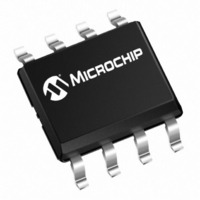
PIC12F510-E/MS Microchip Technology, PIC12F510-E/MS Datasheet - Page 13

PIC12F510-E/MS
Manufacturer Part Number
PIC12F510-E/MS
Description
IC PIC MCU FLASH 1KX14 8MSOP
Manufacturer
Microchip Technology
Series
PIC® 12Fr
Datasheets
1.PIC12F510-ISN.pdf
(124 pages)
2.PIC12F510-ISN.pdf
(8 pages)
3.PIC12F510-ISN.pdf
(20 pages)
Specifications of PIC12F510-E/MS
Core Processor
PIC
Core Size
8-Bit
Speed
8MHz
Peripherals
POR, WDT
Number Of I /o
5
Program Memory Size
1.5KB (1K x 12)
Program Memory Type
FLASH
Ram Size
38 x 8
Voltage - Supply (vcc/vdd)
2 V ~ 5.5 V
Data Converters
A/D 4x8b
Oscillator Type
Internal
Operating Temperature
-40°C ~ 125°C
Package / Case
8-MSOP, Micro8™, 8-uMAX, 8-uSOP,
Processor Series
PIC12F
Core
PIC
Data Bus Width
8 bit
Data Ram Size
38 B
Maximum Clock Frequency
8 MHz
Number Of Programmable I/os
5
Number Of Timers
1
Maximum Operating Temperature
+ 125 C
Mounting Style
SMD/SMT
3rd Party Development Tools
52715-96, 52716-328, 52717-734
Development Tools By Supplier
PG164130, DV164035, DV244005, DV164005, PG164120, DV164101, DV164120, DM163029
Minimum Operating Temperature
- 40 C
On-chip Adc
8 bit, 3 Channel
For Use With
AC162070 - HEADER INTRFC MPLAB ICD2 8/14PAC164325 - MODULE SKT FOR 8MSOP
Lead Free Status / RoHS Status
Lead free / RoHS Compliant
Eeprom Size
-
Connectivity
-
Lead Free Status / Rohs Status
Details
TABLE 3-2:
© 2007 Microchip Technology Inc.
GP0/AN0/C1IN+/ICSPDAT
GP1/AN1/C1IN-/ICSPCLK
GP2/AN2/T0CKI/C1OUT
GP3/MCLR/V
GP4/OSC2
GP5/OSC1/CLKIN
V
V
Legend: I = input, O = output, I/O = input/output, P = power, — = Not Used, TTL = TTL input, ST = Schmitt Trigger
DD
SS
Name
input, AN = Analog Voltage, HV = High Voltage
PP
PIN DESCRIPTIONS – PIC12F510
I/O/P Type
ICSPDAT
ICSPCLK
C1OUT
C1IN+
T0CKI
MCLR
CLKIN
OSC2
OSC1
C1IN-
GP3
GP4
GP0
AN0
GP1
AN1
GP2
AN2
GP5
V
V
V
PP
DD
SS
Input Type
XTAL
TTL
TTL
TTL
TTL
TTL
TTL
AN
AN
AN
AN
AN
HV
ST
ST
ST
ST
ST
—
—
P
P
Output
CMOS
CMOS
CMOS
CMOS
CMOS
CMOS
CMOS
XTAL
Type
—
—
—
—
—
—
—
—
—
—
—
—
—
—
Bidirectional I/O port. Can be software pro-
grammed for internal weak pull-up and wake-up
from Sleep on pin change.
ADC channel input.
Comparator input.
In-Circuit Serial Programming data pin.
Bidirectional I/O port. Can be software pro-
grammed for internal weak pull-up and wake-up
from Sleep on pin change.
ADC channel input.
Comparator input.
In-Circuit Serial Programming clock pin.
Bidirectional I/O port.
ADC channel input.
Timer0 clock input.
Comparator output.
Standard TTL input. Can be software pro-
grammed for internal weak pull-up and wake-up
from Sleep on pin change.
MCLR input – weak pull-up always enabled in
this mode.
Programming Voltage input.
Bidirectional I/O port.
XTAL oscillator output pin.
Bidirectional I/O port.
XTAL oscillator input pin.
EXTRC Schmitt Trigger input.
Positive supply for logic and I/O pins.
Ground reference for logic and I/O pins.
PIC12F510/16F506
Description
DS41268D-page 11


