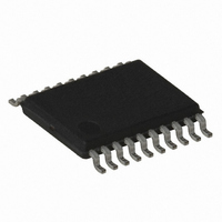
AT89LP2052-20XU Atmel, AT89LP2052-20XU Datasheet - Page 45

AT89LP2052-20XU
Manufacturer Part Number
AT89LP2052-20XU
Description
IC 8051 MCU FLASH 2K 20TSSOP
Manufacturer
Atmel
Series
89LPr
Datasheet
1.AT89LP2052-20PU.pdf
(94 pages)
Specifications of AT89LP2052-20XU
Core Processor
8051
Core Size
8-Bit
Speed
20MHz
Connectivity
SPI, UART/USART
Peripherals
Brown-out Detect/Reset, POR, PWM, WDT
Number Of I /o
15
Program Memory Size
2KB (2K x 8)
Program Memory Type
FLASH
Ram Size
256 x 8
Voltage - Supply (vcc/vdd)
2.4 V ~ 5.5 V
Oscillator Type
Internal
Operating Temperature
-40°C ~ 85°C
Package / Case
20-TSSOP
Processor Series
AT89x
Core
8051
Data Bus Width
8 bit
Data Ram Size
256 B
Interface Type
UART, SPI
Maximum Clock Frequency
20 MHz
Number Of Programmable I/os
15
Number Of Timers
2
Operating Supply Voltage
2.4 V to 5.5 V
Maximum Operating Temperature
+ 85 C
Mounting Style
SMD/SMT
3rd Party Development Tools
PK51, CA51, A51, ULINK2
Development Tools By Supplier
AT89ISP
Minimum Operating Temperature
- 40 C
Lead Free Status / RoHS Status
Lead free / RoHS Compliant
Eeprom Size
-
Data Converters
-
Lead Free Status / Rohs Status
Details
Table 19-1.
Notes:
3547J–MICRO–10/09
SPCR Address = D5H
Not Bit Addressable
Symbol
SPIE
SPE
DORD
MSTR
CPOL
CPHA
SPR0
SPR1
Bit
1. Set up the clock mode before enabling the SPI: set all bits needed in SPCR except the SPE bit, then set SPE.
2. Enable the master SPI prior to the slave device.
3. Slave echoes master on the next Tx if not loaded with new data.
SPIE
SPI interrupt enable. This bit, in conjunction with the ES bit in the IE register, enables SPI interrupts: SPIE = 1 and ES = 1
enable SPI interrupts. SPIE = 0 disables SPI interrupts.
SPI enable. SPE = 1 enables the SPI channel and connects SS, MOSI, MISO and SCK to pins P1.4, P1.5, P1.6, and
P1.7. SPE = 0 disables the SPI channel.
Data order. DORD = 1 selects LSB first data transmission. DORD = 0 selects MSB first data transmission.
Clock polarity. When CPOL = 1, SCK is high when idle. When CPOL = 0, SCK of the master device is low when not
transmitting. Please refer to figure on SPI clock phase and polarity control.
Clock phase. The CPHA bit together with the CPOL bit controls the clock and data relationship between master and
slave. Please refer to figure on SPI clock phase and polarity control.
SPI clock rate select. These two bits control the SCK rate of the device configured as master. SPR1 and SPR0 have no
effect on the slave. The relationship between SCK and the oscillator frequency, F
SPR1
Function
Master/slave select. MSTR = 1 selects Master SPI mode. MSTR = 0 selects slave SPI mode.
7
SPCR – SPI Control Register
0
0
1
1
SPR0
0
1
0
1
SPE
6
SCK
f/4
f/8
f/32
f/64
DORD
5
MSTR
4
CPOL
3
CPHA
2
AT89LP2052/LP4052
OSC.
, is as follows:
Reset Value = 0000 0000B
SPR1
1
SPR0
0
45


