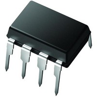
PIC12C672-10E/P Microchip Technology, PIC12C672-10E/P Datasheet - Page 109

PIC12C672-10E/P
Manufacturer Part Number
PIC12C672-10E/P
Description
IC MCU OTP 2KX14 A/D 8DIP
Manufacturer
Microchip Technology
Series
PIC® 12Cr
Datasheets
1.PIC16F688T-ISL.pdf
(688 pages)
2.PIC12CE673-10P.pdf
(129 pages)
3.PIC12CE673-10P.pdf
(14 pages)
Specifications of PIC12C672-10E/P
Core Processor
PIC
Core Size
8-Bit
Speed
10MHz
Peripherals
POR, WDT
Number Of I /o
5
Program Memory Size
3.5KB (2K x 14)
Program Memory Type
OTP
Ram Size
128 x 8
Voltage - Supply (vcc/vdd)
3 V ~ 5.5 V
Data Converters
A/D 4x8b
Oscillator Type
Internal
Operating Temperature
-40°C ~ 125°C
Package / Case
8-DIP (0.300", 7.62mm)
Processor Series
PIC12C
Core
PIC
Data Bus Width
8 bit
Data Ram Size
128 B
Maximum Clock Frequency
10 MHz
Number Of Programmable I/os
5
Number Of Timers
8
Maximum Operating Temperature
+ 125 C
Mounting Style
Through Hole
3rd Party Development Tools
52715-96, 52716-328, 52717-734
Development Tools By Supplier
ICE2000
Minimum Operating Temperature
- 40 C
On-chip Adc
8
Data Rom Size
128 B
Height
3.3 mm
Length
9.27 mm
Supply Voltage (max)
5.5 V
Supply Voltage (min)
3 V
Width
6.35 mm
Lead Free Status / RoHS Status
Lead free / RoHS Compliant
Eeprom Size
-
Connectivity
-
Lead Free Status / Rohs Status
Details
- Current page: 109 of 688
- Download datasheet (3Mb)
1997 Microchip Technology Inc.
Example 6-4: RAM Initialization
Bank0_LP
;
; Next Bank (Bank1)
; (** ONLY REQUIRED IF DEVICE HAS A BANK1 **)
;
Bank1_LP
;
; Next Bank (Bank2)
; (** ONLY REQUIRED IF DEVICE HAS A BANK2 **)
;
Bank2_LP
;
; Next Bank (Bank3)
; (** ONLY REQUIRED IF DEVICE HAS A BANK3 **)
;
Bank3_LP
:
CLRF
MOVLW
MOVWF
CLRF
INCF
BTFSS
GOTO
MOVLW
MOVWF
CLRF
INCF
BTFSS
GOTO
BSF
MOVLW
MOVWF
CLRF
INCF
BTFSS
GOTO
MOVLW
MOVWF
CLRF
INCF
BTFSS
GOTO
Section 6. Memory Organization
STATUS
0x20
FSR
INDF0
FSR
FSR, 7
Bank0_LP
0xA0
FSR
INDF0
FSR
STATUS, C
Bank1_LP
STATUS, IRP
0x20
FSR
INDF0
FSR
FSR, 7
Bank2_LP
0xA0
FSR
INDF0
FSR
STATUS, C
Bank3_LP
; Clear STATUS register (Bank0)
; 1st address (in bank) of GPR area
; Move it to Indirect address register
; Clear GPR at address pointed to by FSR
; Next GPR (RAM) address
; End of current bank ? (FSR = 80h, C = 0)
; NO, clear next location
; 1st address (in bank) of GPR area
; Move it to Indirect address register
; Clear GPR at address pointed to by FSR
; Next GPR (RAM) address
; End of current bank? (FSR = 00h, C = 1)
; NO, clear next location
; Select Bank2 and Bank3
;
; 1st address (in bank) of GPR area
; Move it to Indirect address register
; Clear GPR at address pointed to by FSR
; Next GPR (RAM) address
; End of current bank? (FSR = 80h, C = 0)
; NO, clear next location
; 1st address (in bank) of GPR area
; Move it to Indirect address register
; Clear GPR at address pointed to by FSR
; Next GPR (RAM) address
; End of current bank? (FSR = 00h, C = 1)
; NO, clear next location
; YES, All GPRs (RAM) is cleared
for Indirect addressing
DS31006A-page 6-15
6
Related parts for PIC12C672-10E/P
Image
Part Number
Description
Manufacturer
Datasheet
Request
R

Part Number:
Description:
IC MCU OTP 2KX14 A/D 8DIP
Manufacturer:
Microchip Technology
Datasheet:

Part Number:
Description:
IC MCU OTP 2KX14 A/D 8-SOIJ
Manufacturer:
Microchip Technology
Datasheet:

Part Number:
Description:
IC MCU OTP 2KX14 A/D 8-SOIJ
Manufacturer:
Microchip Technology
Datasheet:

Part Number:
Description:
IC MCU OTP 2KX14 A/D 8-SOIJ
Manufacturer:
Microchip Technology
Datasheet:

Part Number:
Description:
IC MCU OTP 2KX14 A/D 8DIP
Manufacturer:
Microchip Technology
Datasheet:

Part Number:
Description:
IC MCU OTP 2KX14 A/D 8-SOIJ
Manufacturer:
Microchip Technology
Datasheet:

Part Number:
Description:
IC MCU OTP 2KX14 A/D 8DFN
Manufacturer:
Microchip Technology
Datasheet:

Part Number:
Description:
IC PIC MCU 2KX14 8DFN
Manufacturer:
Microchip Technology
Datasheet:

Part Number:
Description:
IC MCU OTP 2KX14 A/D 8-SOIJ
Manufacturer:
Microchip Technology
Datasheet:

Part Number:
Description:
IC MCU OTP 2KX14 A/D 8DFN
Manufacturer:
Microchip Technology
Datasheet:

Part Number:
Description:
IC MCU OTP 2KX14 A/D 8DIP
Manufacturer:
Microchip Technology
Datasheet:

Part Number:
Description:
IC MCU OTP 2KX14 A/D 8-SOIJ
Manufacturer:
Microchip Technology
Datasheet:

Part Number:
Description:
IC MCU EPROM 2KX14 A/D 8CDIP
Manufacturer:
Microchip Technology
Datasheet:

Part Number:
Description:
IC,MICROCONTROLLER,8-BIT,PIC CPU,CMOS,DIP,8PIN,PLASTIC
Manufacturer:
Microchip Technology
Datasheet:

Part Number:
Description:
IC,MICROCONTROLLER,8-BIT,PIC CPU,CMOS,DIP,8PIN,PLASTIC
Manufacturer:
Microchip Technology
Datasheet:


