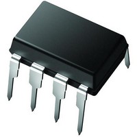
PIC12C672-10E/P Microchip Technology, PIC12C672-10E/P Datasheet - Page 389

PIC12C672-10E/P
Manufacturer Part Number
PIC12C672-10E/P
Description
IC MCU OTP 2KX14 A/D 8DIP
Manufacturer
Microchip Technology
Series
PIC® 12Cr
Datasheets
1.PIC16F688T-ISL.pdf
(688 pages)
2.PIC12CE673-10P.pdf
(129 pages)
3.PIC12CE673-10P.pdf
(14 pages)
Specifications of PIC12C672-10E/P
Core Processor
PIC
Core Size
8-Bit
Speed
10MHz
Peripherals
POR, WDT
Number Of I /o
5
Program Memory Size
3.5KB (2K x 14)
Program Memory Type
OTP
Ram Size
128 x 8
Voltage - Supply (vcc/vdd)
3 V ~ 5.5 V
Data Converters
A/D 4x8b
Oscillator Type
Internal
Operating Temperature
-40°C ~ 125°C
Package / Case
8-DIP (0.300", 7.62mm)
Processor Series
PIC12C
Core
PIC
Data Bus Width
8 bit
Data Ram Size
128 B
Maximum Clock Frequency
10 MHz
Number Of Programmable I/os
5
Number Of Timers
8
Maximum Operating Temperature
+ 125 C
Mounting Style
Through Hole
3rd Party Development Tools
52715-96, 52716-328, 52717-734
Development Tools By Supplier
ICE2000
Minimum Operating Temperature
- 40 C
On-chip Adc
8
Data Rom Size
128 B
Height
3.3 mm
Length
9.27 mm
Supply Voltage (max)
5.5 V
Supply Voltage (min)
3 V
Width
6.35 mm
Lead Free Status / RoHS Status
Lead free / RoHS Compliant
Eeprom Size
-
Connectivity
-
Lead Free Status / Rohs Status
Details
- Current page: 389 of 688
- Download datasheet (3Mb)
21.3
1997 Microchip Technology Inc.
Operation
When the A/D conversion is complete, the result is loaded into the ADRES register, the
GO/DONE bit (ADCON0<2>) is cleared, and A/D interrupt flag bit, ADIF, is set.
After the A/D module has been configured as desired, the selected channel must be acquired
before the conversion is started. The analog input channels must have their corresponding TRIS
bits selected as an input. To determine acquisition time, see Subsection
Requirements.”
following steps should be followed for doing an A/D conversion:
1.
2.
3.
4.
5.
6.
7.
Figure 21-2
time that the A/D module’s holding capacitor is connected to the external voltage level. Then
there is the conversion time of 10 T
two times is the sampling time. There is a minimum acquisition time to ensure that the holding
capacitor is charged to a level that will give the desired accuracy for the A/D conversion.
Figure 21-2: A/D Conversion Sequence
Configure the A/D module:
• Configure analog pins / voltage reference / and digital I/O (ADCON1)
• Select A/D input channel (ADCON0)
• Select A/D conversion clock (ADCON0)
• Turn on A/D module (ADCON0)
Configure A/D interrupt (if desired):
• Clear the ADIF bit
• Set the ADIE bit
• Set the GIE bit
Wait the required acquisition time.
Start conversion:
• Set the GO/DONE bit (ADCON0)
Wait for A/D conversion to complete, by either:
• Polling for the GO/DONE bit to be cleared
OR
• Waiting for the A/D interrupt
Read A/D Result register (ADRES), clear the ADIF bit, if required.
For next conversion, go to step 1 or step 2 as required. The A/D conversion time per bit is
defined as T
When A/D holding capacitor start to charge.
After A/D conversion, or new A/D channel is selected.
Acquisition Time
shows the conversion sequence, and the terms that are used. Acquisition time is the
Section 21. 8-bit A/D Converter
AD
After this acquisition time has elapsed the A/D conversion can be started. The
. A minimum wait of 2T
A/D Sample Time
When A/D conversion is started (setting the GO bit).
Holding capacitor is disconnected from the analog input before
the conversion is started.
Conversion Time
AD
, which is started when the GO bit is set. The sum of these
AD
is required before next acquisition starts.
A/D conversion complete,
result is loaded in ADRES register.
Holding capacitor begins acquiring
voltage level on selected channel.
ADIF bit is set.
21.4 “A/D Acquisition
DS31021A-page 21-5
21
Related parts for PIC12C672-10E/P
Image
Part Number
Description
Manufacturer
Datasheet
Request
R

Part Number:
Description:
IC MCU OTP 2KX14 A/D 8DIP
Manufacturer:
Microchip Technology
Datasheet:

Part Number:
Description:
IC MCU OTP 2KX14 A/D 8-SOIJ
Manufacturer:
Microchip Technology
Datasheet:

Part Number:
Description:
IC MCU OTP 2KX14 A/D 8-SOIJ
Manufacturer:
Microchip Technology
Datasheet:

Part Number:
Description:
IC MCU OTP 2KX14 A/D 8-SOIJ
Manufacturer:
Microchip Technology
Datasheet:

Part Number:
Description:
IC MCU OTP 2KX14 A/D 8DIP
Manufacturer:
Microchip Technology
Datasheet:

Part Number:
Description:
IC MCU OTP 2KX14 A/D 8-SOIJ
Manufacturer:
Microchip Technology
Datasheet:

Part Number:
Description:
IC MCU OTP 2KX14 A/D 8DFN
Manufacturer:
Microchip Technology
Datasheet:

Part Number:
Description:
IC PIC MCU 2KX14 8DFN
Manufacturer:
Microchip Technology
Datasheet:

Part Number:
Description:
IC MCU OTP 2KX14 A/D 8-SOIJ
Manufacturer:
Microchip Technology
Datasheet:

Part Number:
Description:
IC MCU OTP 2KX14 A/D 8DFN
Manufacturer:
Microchip Technology
Datasheet:

Part Number:
Description:
IC MCU OTP 2KX14 A/D 8DIP
Manufacturer:
Microchip Technology
Datasheet:

Part Number:
Description:
IC MCU OTP 2KX14 A/D 8-SOIJ
Manufacturer:
Microchip Technology
Datasheet:

Part Number:
Description:
IC MCU EPROM 2KX14 A/D 8CDIP
Manufacturer:
Microchip Technology
Datasheet:

Part Number:
Description:
IC,MICROCONTROLLER,8-BIT,PIC CPU,CMOS,DIP,8PIN,PLASTIC
Manufacturer:
Microchip Technology
Datasheet:

Part Number:
Description:
IC,MICROCONTROLLER,8-BIT,PIC CPU,CMOS,DIP,8PIN,PLASTIC
Manufacturer:
Microchip Technology
Datasheet:


