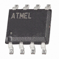
ATTINY25V-15ST Atmel, ATTINY25V-15ST Datasheet - Page 118

ATTINY25V-15ST
Manufacturer Part Number
ATTINY25V-15ST
Description
MCU AVR 2K FLASH 4MHZ 8-SOIC
Manufacturer
Atmel
Series
AVR® ATtinyr
Datasheet
1.ATTINY25-15MZ.pdf
(196 pages)
Specifications of ATTINY25V-15ST
Package / Case
8-SOIC (3.9mm Width)
Voltage - Supply (vcc/vdd)
1.8 V ~ 3.6 V
Operating Temperature
-40°C ~ 85°C
Speed
8MHz
Number Of I /o
6
Eeprom Size
128 x 8
Core Processor
AVR
Program Memory Type
FLASH
Ram Size
128 x 8
Program Memory Size
2KB (2K x 8)
Data Converters
A/D 4x10b
Oscillator Type
Internal
Peripherals
Brown-out Detect/Reset, POR, PWM, WDT
Connectivity
USI
Core Size
8-Bit
Processor Series
ATTINY2x
Core
AVR8
Data Bus Width
8 bit
Data Ram Size
128 B
Maximum Operating Temperature
+ 85 C
Mounting Style
SMD/SMT
Lead Free Status / RoHS Status
Lead free / RoHS Compliant
Available stocks
Company
Part Number
Manufacturer
Quantity
Price
Part Number:
ATTINY25V-15ST
Manufacturer:
ATMEL/爱特梅尔
Quantity:
20 000
- Current page: 118 of 196
- Download datasheet (4Mb)
18.5.2
18.6
18.6.1
118
ADC Noise Canceler
ATtiny25/45/85
ADC Voltage Reference
Analog Input Circuitry
The voltage reference for the ADC (V
ended channels that exceed V
either V
version result after switching voltage reference source may be inaccurate, and the user is
advised to discard this result.
The ADC features a noise canceler that enables conversion during sleep mode to reduce noise
induced from the CPU core and other I/O peripherals. The noise canceler can be used with ADC
Noise Reduction and Idle mode. To make use of this feature, the following procedure should be
used:
Note that the ADC will not be automatically turned off when entering other sleep modes than Idle
mode and ADC Noise Reduction mode. The user is advised to write zero to ADEN before enter-
ing such sleep modes to avoid excessive power consumption.
The analog input circuitry for single ended channels is illustrated in Figure 18-8. An analog
source applied to ADCn is subjected to the pin capacitance and input leakage of that pin, regard-
less of whether that channel is selected as input for the ADC. When the channel is selected, the
source must drive the S/H capacitor through the series resistance (combined resistance in the
input path).
The ADC is optimized for analog signals with an output impedance of approximately 10 k or
less. If such a source is used, the sampling time will be negligible. If a source with higher imped-
ance is used, the sampling time will depend on how long time the source needs to charge the
S/H capacitor, with can vary widely. The user is recommended to only use low impedant sources
with slowly varying signals, since this minimizes the required charge transfer to the S/H
capacitor.
Signal components higher than the Nyquist frequency (f
distortion from unpredictable signal convolution. The user is advised to remove high frequency
components with a low-pass filter before applying the signals as inputs to the ADC.
a. Make sure that the ADC is enabled and is not busy converting. Single Conversion
b. Enter ADC Noise Reduction mode (or Idle mode). The ADC will start a conversion
c. If no other interrupts occur before the ADC conversion completes, the ADC inter-
CC
mode must be selected and the ADC conversion complete interrupt must be
enabled.
once the CPU has been halted.
rupt will wake up the CPU and execute the ADC Conversion Complete interrupt
routine. If another interrupt wakes up the CPU before the ADC conversion is com-
plete, that interrupt will be executed, and an ADC Conversion Complete interrupt
request will be generated when the ADC conversion completes. The CPU will
remain in active mode until a new sleep command is executed.
, or internal 1.1V / 2.56V voltage reference, or external AREF pin. The first ADC con-
REF
will result in codes close to 0x3FF. V
REF
) indicates the conversion range for the ADC. Single
ADC
/2) should not be present to avoid
REF
can be selected as
7598H–AVR–07/09
Related parts for ATTINY25V-15ST
Image
Part Number
Description
Manufacturer
Datasheet
Request
R

Part Number:
Description:
IC MCU AVR 2K FLASH 10MHZ 20-QFN
Manufacturer:
Atmel
Datasheet:

Part Number:
Description:
MCU AVR 2KB FLASH 10MHZ 8SOIC
Manufacturer:
Atmel
Datasheet:

Part Number:
Description:
IC AVR MCU 2K 10MHZ 8-DIP
Manufacturer:
Atmel
Datasheet:

Part Number:
Description:
IC MCU AVR 2KB FLASH 10MHZ 8SOIC
Manufacturer:
Atmel
Datasheet:

Part Number:
Description:
IC MCU AVR 2KB FLASH 10MHZ 8SOIC
Manufacturer:
Atmel
Datasheet:

Part Number:
Description:
MCU AVR 2KB FLASH 10MHZ 8SOIC
Manufacturer:
Atmel
Datasheet:

Part Number:
Description:
MCU AVR 2KB FLASH 10MHZ 20QFN
Manufacturer:
Atmel
Datasheet:

Part Number:
Description:
MCU AVR 2K ISP FLASH 1.8V 8-SOIC
Manufacturer:
Atmel
Datasheet:

Part Number:
Description:
IC AVR MCU 2K 10MHZ 8DIP
Manufacturer:
Atmel
Datasheet:

Part Number:
Description:
IC AVR MCU 2K 10MHZ 8SOIC
Manufacturer:
Atmel
Datasheet:

Part Number:
Description:
8-bit Microcontrollers - MCU 2KB FLASH,128B EE, 128B SRAM-10MHz
Manufacturer:
Atmel

Part Number:
Description:
8-bit Microcontrollers - MCU 2KB FL,128B EE,128B SRAM-10MHz
Manufacturer:
Atmel

Part Number:
Description:
8-bit Microcontrollers - MCU AVR 16KB FL 512B EE 1KB SRAM 10 MHZ GRN
Manufacturer:
Atmel


