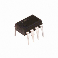
ATTINY45-20PU Atmel, ATTINY45-20PU Datasheet - Page 97

ATTINY45-20PU
Manufacturer Part Number
ATTINY45-20PU
Description
IC AVR MCU 4K 20MHZ 8DIP
Manufacturer
Atmel
Series
AVR® ATtinyr
Specifications of ATTINY45-20PU
Core Processor
AVR
Core Size
8-Bit
Speed
20MHz
Connectivity
USI
Peripherals
Brown-out Detect/Reset, POR, PWM, WDT
Number Of I /o
6
Program Memory Size
4KB (2K x 16)
Program Memory Type
FLASH
Eeprom Size
256 x 8
Ram Size
256 x 8
Voltage - Supply (vcc/vdd)
2.7 V ~ 5.5 V
Data Converters
A/D 4x10b
Oscillator Type
Internal
Operating Temperature
-40°C ~ 85°C
Package / Case
8-DIP (0.300", 7.62mm)
Processor Series
ATTINY4x
Core
AVR8
Data Bus Width
8 bit
Data Ram Size
256 B
Interface Type
USI
Maximum Clock Frequency
10 MHz
Number Of Programmable I/os
6
Number Of Timers
2
Operating Supply Voltage
2.7 V to 5.5 V
Maximum Operating Temperature
+ 85 C
Mounting Style
Through Hole
3rd Party Development Tools
EWAVR, EWAVR-BL
Development Tools By Supplier
ATAVRDRAGON, ATSTK500, ATSTK600, ATAVRISP2, ATAVRONEKIT
Minimum Operating Temperature
- 40 C
On-chip Adc
10 bit, 4 Channel
Package
8PDIP
Device Core
AVR
Family Name
ATtiny
Maximum Speed
20 MHz
For Use With
ATSTK600-DIP40 - STK600 SOCKET/ADAPTER 40-PDIPATAVRBC100 - REF DESIGN KIT BATTERY CHARGER770-1007 - ISP 4PORT ATMEL AVR MCU SPI/JTAGATAVRDRAGON - KIT DRAGON 32KB FLASH MEM AVRATAVRISP2 - PROGRAMMER AVR IN SYSTEMATJTAGICE2 - AVR ON-CHIP D-BUG SYSTEM
Lead Free Status / RoHS Status
Lead free / RoHS Compliant
Available stocks
Company
Part Number
Manufacturer
Quantity
Price
Company:
Part Number:
ATTINY45-20PU
Manufacturer:
ATMEL
Quantity:
3 000
Company:
Part Number:
ATTINY45-20PU
Manufacturer:
ATMEL
Quantity:
6 500
Company:
Part Number:
ATTINY45-20PU
Manufacturer:
Atmel
Quantity:
55 609
12.3.9
2586M–AVR–07/10
PLLCSR – PLL Control and Status Register
• Bit 2 – TOV1: Timer/Counter1 Overflow Flag
In normal mode (PWM1A=0 and PWM1B=0) the bit TOV1 is set (one) when an overflow occurs
in Timer/Counter1. The bit TOV1 is cleared by hardware when executing the corresponding
interrupt handling vector. Alternatively, TOV1 is cleared, after synchronization clock cycle, by
writing a logical one to the flag.
In PWM mode (either PWM1A=1 or PWM1B=1) the bit TOV1 is set (one) when compare match
occurs between Timer/Counter1 and data value in OCR1C - Output Compare Register 1C.
When the SREG I-bit, and TOIE1 (Timer/Counter1 Overflow Interrupt Enable), and TOV1 are set
(one), the Timer/Counter1 Overflow interrupt is executed.
• Bit 0 – Res: Reserved Bit
This bit is a reserved bit in the ATtiny25/45/85 and always reads as zero.
• Bit 7 – LSM: Low Speed Mode
The high speed mode is enabled as default and the fast peripheral clock is 64 MHz, but the low
speed mode can be set by writing the LSM bit to one. Then the fast peripheral clock is scaled
down to 32 MHz. The low speed mode must be set, if the supply voltage is below 2.7 volts,
because the Timer/Counter1 is not running fast enough on low voltage levels. It is highly recom-
mended that Timer/Counter1 is stopped whenever the LSM bit is changed.
Note, that LSM can not be set if PLL
• Bit 6:3 – Res : Reserved Bits
These bits are reserved bits in the ATtiny25/45/85 and always read as zero.
• Bit 2 – PCKE: PCK Enable
The PCKE bit change the Timer/Counter1 clock source. When it is set, the asynchronous clock
mode is enabled and fast 64 MHz (or 32 MHz in Low Speed Mode) PCK clock is used as
Timer/Counter1 clock source. If this bit is cleared, the synchronous clock mode is enabled, and
system clock CK is used as Timer/Counter1 clock source. This bit can be set only if PLLE bit is
set. It is safe to set this bit only when the PLL is locked i.e the PLOCK bit is 1. The bit PCKE can
only be set, if the PLL has been enabled earlier.
• Bit 1 – PLLE: PLL Enable
When the PLLE is set, the PLL is started and if needed internal RC-oscillator is started as a PLL
reference clock. If PLL is selected as a system clock source the value for this bit is always 1.
• Bit 0 – PLOCK: PLL Lock Detector
When the PLOCK bit is set, the PLL is locked to the reference clock. The PLOCK bit should be
ignored during initial PLL lock-in sequence when PLL frequency overshoots and undershoots,
before reaching steady state. The steady state is obtained within 100 µs. After PLL lock-in it is
recommended to check the PLOCK bit before enabling PCK for Timer/Counter1.
Bit
0x27
Read/Write
Initial value
LSM
R/W
7
0
R
6
0
-
R
5
0
-
CLK
is used as system clock.
R
4
0
-
R
3
0
-
PCKE
R/W
2
0
PLLE
R/W
0/1
1
PLOCK
R
0
0
PLLCSR
97


