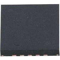
ATTINY25-15MZ Atmel, ATTINY25-15MZ Datasheet - Page 22

ATTINY25-15MZ
Manufacturer Part Number
ATTINY25-15MZ
Description
MCU AVR 2K FLASH 15MHZ 20-QFN
Manufacturer
Atmel
Series
AVR® ATtinyr
Datasheet
1.ATTINY25-15MZ.pdf
(196 pages)
Specifications of ATTINY25-15MZ
Package / Case
20-QFN
Voltage - Supply (vcc/vdd)
2.7 V ~ 5.5 V
Operating Temperature
-40°C ~ 125°C
Speed
16MHz
Number Of I /o
6
Eeprom Size
128 x 8
Core Processor
AVR
Program Memory Type
FLASH
Ram Size
128 x 8
Program Memory Size
2KB (2K x 8)
Data Converters
A/D 4x10b
Oscillator Type
Internal
Peripherals
Brown-out Detect/Reset, POR, PWM, WDT
Connectivity
USI
Core Size
8-Bit
Processor Series
ATTINY2x
Core
AVR8
Data Bus Width
8 bit
Data Ram Size
128 B
Interface Type
UART, SPI, USI
Maximum Clock Frequency
16 MHz
Number Of Programmable I/os
6
Number Of Timers
2
Maximum Operating Temperature
+ 85 C
Mounting Style
SMD/SMT
3rd Party Development Tools
EWAVR, EWAVR-BL
Development Tools By Supplier
ATAVRDRAGON, ATSTK500, ATSTK600, ATAVRISP2, ATAVRONEKIT
Minimum Operating Temperature
- 40 C
On-chip Adc
10 bit, 4 Channel
Data Rom Size
128 B
A/d Bit Size
10 bit
A/d Channels Available
4
Height
0.75 mm
Length
4 mm
Supply Voltage (max)
5.5 V
Supply Voltage (min)
2.7 V
Width
4 mm
Lead Free Status / RoHS Status
Lead free / RoHS Compliant
- Current page: 22 of 196
- Download datasheet (4Mb)
6.1.1
6.1.2
6.1.3
6.1.4
6.1.5
22
ATtiny25/45/85
CPU Clock – clk
I/O Clock – clk
Flash Clock – clk
ADC Clock – clk
Internal PLL for Fast Peripheral Clock Generation - clk
I/O
The CPU clock is routed to parts of the system concerned with operation of the AVR core.
Examples of such modules are the General Purpose Register File, the Status Register and the
Data memory holding the Stack Pointer. Halting the CPU clock inhibits the core from performing
general operations and calculations.
The I/O clock is used by the majority of the I/O modules, like Timer/Counter. The I/O clock is
also used by the External Interrupt module, but note that some external interrupts are detected
by asynchronous logic, allowing such interrupts to be detected even if the I/O clock is halted.
The Flash clock controls operation of the Flash interface. The Flash clock is usually active simul-
taneously with the CPU clock.
The ADC is provided with a dedicated clock domain. This allows halting the CPU and I/O clocks
in order to reduce noise generated by digital circuitry. This gives more accurate ADC conversion
results.
The internal PLL in ATtiny25/45/85 generates a clock frequency that is 8x multiplied from a
source input. The source of the PLL input clock is the output of the internal RC oscillator having
a frequency of 8.0 MHz. Thus the output of the PLL, the fast peripheral clock is 64 MHz. The fast
peripheral clock, or a clock prescaled from that, can be selected as the clock source for
Timer/Counter1. See the
The PLL is locked on the RC oscillator and adjusting the RC oscillator via OSCCAL register will
adjust the fast peripheral clock at the same time. However, even if the RC oscillator is taken to a
higher frequency than 8 MHz, the fast peripheral clock frequency saturates at 85 MHz (worst
case) and remains oscillating at the maximum frequency. It should be noted that the PLL in this
case is not locked any longer with the RC oscillator clock.
Therefore, it is recommended not to take the OSCCAL adjustments to a higher frequency than 8
MHz in order to keep the PLL in the correct operating range. The internal PLL is enabled only
when the PLLE bit in PLLCSR is set or the PLLCK fuse is programmed (‘0’). The bit PLOCK
from PLLCSR is set when PLL is locked.
Both internal RC oscillator and PLL are switched off in power down and stand-by sleep modes.
CPU
ADC
FLASH
Figure 6-2 on page
PCK
23.
7598H–AVR–07/09
Related parts for ATTINY25-15MZ
Image
Part Number
Description
Manufacturer
Datasheet
Request
R

Part Number:
Description:
Manufacturer:
Atmel Corporation
Datasheet:

Part Number:
Description:
Manufacturer:
Atmel Corporation
Datasheet:

Part Number:
Description:
IC MCU AVR 2K FLASH 20MHZ 20-QFN
Manufacturer:
Atmel
Datasheet:

Part Number:
Description:
IC AVR MCU 2K 20MHZ 8-DIP
Manufacturer:
Atmel
Datasheet:

Part Number:
Description:
IC AVR MCU 2K 20MHZ 8-SOIC
Manufacturer:
Atmel
Datasheet:

Part Number:
Description:
8-bit Microcontrollers - MCU AVR 16KB FL 512B EE 1KB SRAM 10 MHZ GRN
Manufacturer:
Atmel

Part Number:
Description:
8-bit Microcontrollers - MCU AVR 16KB FL 512B EE 1KB SRAM 10 MHZ GRN
Manufacturer:
Atmel

Part Number:
Description:
MCU AVR 2K ISP FLASH 2.7V 8-SOIC
Manufacturer:
Atmel
Datasheet:

Part Number:
Description:
MCU AVR 2KB FLASH 20MHZ 8SOIC
Manufacturer:
Atmel
Datasheet:

Part Number:
Description:
IC MCU AVR 2KB FLASH 20MHZ 8SOIC
Manufacturer:
Atmel
Datasheet:

Part Number:
Description:
IC MCU AVR 2KB FLASH 20MHZ 8SOIC
Manufacturer:
Atmel
Datasheet:

Part Number:
Description:
MCU AVR 2KB FLASH 20MHZ 8SOIC
Manufacturer:
Atmel
Datasheet:

Part Number:
Description:
MCU AVR 2KB FLASH 20MHZ 8SOIC
Manufacturer:
Atmel
Datasheet:

Part Number:
Description:
MCU AVR 2KB FLASH 20MHZ 20QFN
Manufacturer:
Atmel
Datasheet:


