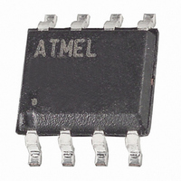
ATTINY45-15SZ Atmel, ATTINY45-15SZ Datasheet - Page 18

ATTINY45-15SZ
Manufacturer Part Number
ATTINY45-15SZ
Description
MCU AVR 4K FLASH 15MHZ 8-SOIC
Manufacturer
Atmel
Series
AVR® ATtinyr
Datasheet
1.ATTINY25-15MZ.pdf
(196 pages)
Specifications of ATTINY45-15SZ
Package / Case
8-SOIC (3.9mm Width)
Voltage - Supply (vcc/vdd)
2.7 V ~ 5.5 V
Operating Temperature
-40°C ~ 125°C
Speed
16MHz
Number Of I /o
6
Eeprom Size
256 x 8
Core Processor
AVR
Program Memory Type
FLASH
Ram Size
256 x 8
Program Memory Size
4KB (4K x 8)
Data Converters
A/D 4x10b
Oscillator Type
Internal
Peripherals
Brown-out Detect/Reset, POR, PWM, WDT
Connectivity
USI
Core Size
8-Bit
Lead Free Status / RoHS Status
Lead free / RoHS Compliant
Available stocks
Company
Part Number
Manufacturer
Quantity
Price
Part Number:
ATTINY45-15SZ
Manufacturer:
ATMEL/爱特梅尔
Quantity:
20 000
- Current page: 18 of 196
- Download datasheet (4Mb)
5.3.6
5.3.7
5.3.8
5.3.9
18
ATtiny25/45/85
Atomic Byte Programming
Split Byte Programming
Erase
Write
Using Atomic Byte Programming is the simplest mode. When writing a byte to the EEPROM, the
user must write the address into the EEAR Register and data into EEDR Register. If the EEPMn
bits are zero, writing EEPE (within four cycles after EEMPE is written) will trigger the erase/write
operation. Both the erase and write cycle are done in one operation and the total programming
time is given in
completed. While the device is busy with programming, it is not possible to do any other
EEPROM operations.
It is possible to split the erase and write cycle in two different operations. This may be useful if
the system requires short access time for some limited period of time (typically if the power sup-
ply voltage falls). In order to take advantage of this method, it is required that the locations to be
written have been erased before the write operation. But since the erase and write operations
are split, it is possible to do the erase operations when the system allows doing time-critical
operations (typically after Power-up).
To erase a byte, the address must be written to EEAR. If the EEPMn bits are 0b01, writing the
EEPE (within four cycles after EEMPE is written) will trigger the erase operation only (program-
ming time is given in
While the device is busy programming, it is not possible to do any other EEPROM operations.
To write a location, the user must write the address into EEAR and the data into EEDR. If the
EEPMn bits are 0b10, writing the EEPE (within four cycles after EEMPE is written) will trigger
the write operation only (programming time is given in
until the write operation completes. If the location to be written has not been erased before write,
the data that is stored must be considered as lost. While the device is busy with programming, it
is not possible to do any other EEPROM operations.
The calibrated Oscillator is used to time the EEPROM accesses. Make sure the Oscillator fre-
quency is within the requirements described in
page
The following code examples show one assembly and one C function for erase, write, or atomic
write of the EEPROM. The examples assume that interrupts are controlled (e.g., by disabling
interrupts globally) so that no interrupts will occur during execution of these functions
26.
Table
Table
20-1. The EEPE bit remains set until the erase and write operations are
20-1). The EEPE bit remains set until the erase operation completes.
“Oscillator Calibration Register – OSCCAL” on
Table
20-1). The EEPE bit remains set
7598H–AVR–07/09
Related parts for ATTINY45-15SZ
Image
Part Number
Description
Manufacturer
Datasheet
Request
R

Part Number:
Description:
Manufacturer:
Atmel Corporation
Datasheet:

Part Number:
Description:
Manufacturer:
Atmel Corporation
Datasheet:

Part Number:
Description:
IC AVR MCU 4K 20MHZ 8SOIC
Manufacturer:
Atmel
Datasheet:

Part Number:
Description:
IC AVR MCU 4K 20MHZ 8DIP
Manufacturer:
Atmel
Datasheet:

Part Number:
Description:
MCU AVR 4KB FLASH 20MHZ 8SOIC
Manufacturer:
Atmel
Datasheet:

Part Number:
Description:
IC MCU AVR 4K FLASH 20MHZ 8TSSOP
Manufacturer:
Atmel
Datasheet:

Part Number:
Description:
IC AVR MCU FLASH 4K 20MHZ 20MLF
Manufacturer:
Atmel
Datasheet:

Part Number:
Description:
MCU AVR 4KB FLASH 20MHZ 8TSSOP
Manufacturer:
Atmel
Datasheet:

Part Number:
Description:
IC MCU AVR 4KB FLASH 20MHZ 8SOIC
Manufacturer:
Atmel
Datasheet:

Part Number:
Description:
MCU AVR 4KB FLASH 20MHZ 20QFN
Manufacturer:
Atmel
Datasheet:


