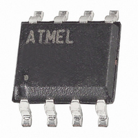
ATTINY45-15SZ Atmel, ATTINY45-15SZ Datasheet - Page 54

ATTINY45-15SZ
Manufacturer Part Number
ATTINY45-15SZ
Description
MCU AVR 4K FLASH 15MHZ 8-SOIC
Manufacturer
Atmel
Series
AVR® ATtinyr
Datasheet
1.ATTINY25-15MZ.pdf
(196 pages)
Specifications of ATTINY45-15SZ
Package / Case
8-SOIC (3.9mm Width)
Voltage - Supply (vcc/vdd)
2.7 V ~ 5.5 V
Operating Temperature
-40°C ~ 125°C
Speed
16MHz
Number Of I /o
6
Eeprom Size
256 x 8
Core Processor
AVR
Program Memory Type
FLASH
Ram Size
256 x 8
Program Memory Size
4KB (4K x 8)
Data Converters
A/D 4x10b
Oscillator Type
Internal
Peripherals
Brown-out Detect/Reset, POR, PWM, WDT
Connectivity
USI
Core Size
8-Bit
Lead Free Status / RoHS Status
Lead free / RoHS Compliant
Available stocks
Company
Part Number
Manufacturer
Quantity
Price
Part Number:
ATTINY45-15SZ
Manufacturer:
ATMEL/爱特梅尔
Quantity:
20 000
- Current page: 54 of 196
- Download datasheet (4Mb)
10.3.1
10.3.2
54
ATtiny25/45/85
MCU Control Register – MCUCR
Alternate Functions of Port B
• Bit 6 – PUD: Pull-up Disable
When this bit is written to one, the pull-ups in the I/O ports are disabled even if the DDxn and
PORTxn Registers are configured to enable the pull-ups ({DDxn, PORTxn} = 0b01). See
figuring the Pin” on page 48
The Port B pins with alternate function are shown in
Table 10-3.
Notes:
• Port B, Bit 5 - RESET/dW/ADC0/PCINT5
RESET: External Reset input is active low and enabled by unprogramming (“1”) the RSTDISBL
Fuse. Pullup is activated and output driver and digital input are deactivated when the pin is used
as the RESET pin.
dW: When the debugWIRE Enable (DWEN) Fuse is programmed and Lock bits are unpro-
grammed, the debugWIRE system within the target device is activated. The RESET port pin is
configured as a wire-AND (open-drain) bi-directional I/O pin with pull-up enabled and becomes
the communication gateway between target and emulator.
ADC0: Analog to Digital Converter, Channel 0
PCINT5: Pin Change Interrupt source 5.
Bit
Read/Write
Initial Value
1. Reset Pin, debugWIRE I/O, ADC Input Channel or Pin Change Interrupt.
2. XOSC Output, Divided System Clock Output, ADC Input Channel, Timer/Counter1 Output
3. XOSC Input / External Clock Input, ADC Input Channel, Timer/Counter1 Inverted Output Com-
4. Serial Clock Input, ADC Input Channel, Timer/Counter Clock Input, USI Clock (three-wire
5. Serial Data Input, Analog Comparator Negative Input, Timer/Counter0 Output Compare and
6. Serial Data Output, Analog Comparator Positive Input, Timer/Counter0 Output Compare and
Port Pin
Compare and PWM Output B, or Pin Change Interrupt.
pare and PWM Output B, or Pin Change Interrupt.
mode), USI Clock (two-wire mode), External Interrupt, or Pin Change Interrupt.
PWM Output B, Timer/Counter1 Output Compare and PWM Output A, USI Data Output
(three-wire mode), or Pin Change Interrupt.
PWM Output A, Timer/Counter1 Inverted Output Compare and PWM Output A, USI Data Input
(three-wire mode), USI Data (two-wire mode), Voltage Ref., or Pin Change Interrupt.
PB5
PB4
PB3
PB2
PB1
PB0
BODS
Port B Pins Alternate Functions
R/W
7
0
PUD
R/W
6
0
for more details about this feature.
Alternate Function
RESET / dW / ADC0 / PCINT5
XTAL2 / CLKO / ADC2 / OC1B / PCINT4
XTAL1 / ADC3 / OC1B / PCINT3
SCK / ADC1 / T0 / USCK / SCL / INT0 / PCINT2
MISO / AIN1 / OC0B / OC1A / DO / PCINT1
MOSI / AIN0 / OC0A / OC1A / DI / SDA / AREF / PCINT0
R/W
SE
5
0
SM1
R/W
4
0
.
Table
SM0
R/W
3
0
(1)
(3)
10-3.
BODSE
R/W
2
0
(2)
(5)
ISC01
R/W
(4)
1
0
ISC00
(6)
R/W
0
0
7598H–AVR–07/09
MCUCR
“Con-
Related parts for ATTINY45-15SZ
Image
Part Number
Description
Manufacturer
Datasheet
Request
R

Part Number:
Description:
Manufacturer:
Atmel Corporation
Datasheet:

Part Number:
Description:
Manufacturer:
Atmel Corporation
Datasheet:

Part Number:
Description:
IC AVR MCU 4K 20MHZ 8SOIC
Manufacturer:
Atmel
Datasheet:

Part Number:
Description:
IC AVR MCU 4K 20MHZ 8DIP
Manufacturer:
Atmel
Datasheet:

Part Number:
Description:
MCU AVR 4KB FLASH 20MHZ 8SOIC
Manufacturer:
Atmel
Datasheet:

Part Number:
Description:
IC MCU AVR 4K FLASH 20MHZ 8TSSOP
Manufacturer:
Atmel
Datasheet:

Part Number:
Description:
IC AVR MCU FLASH 4K 20MHZ 20MLF
Manufacturer:
Atmel
Datasheet:

Part Number:
Description:
MCU AVR 4KB FLASH 20MHZ 8TSSOP
Manufacturer:
Atmel
Datasheet:

Part Number:
Description:
IC MCU AVR 4KB FLASH 20MHZ 8SOIC
Manufacturer:
Atmel
Datasheet:

Part Number:
Description:
MCU AVR 4KB FLASH 20MHZ 20QFN
Manufacturer:
Atmel
Datasheet:


