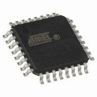
AT90USB162-16AU Atmel, AT90USB162-16AU Datasheet - Page 259

AT90USB162-16AU
Manufacturer Part Number
AT90USB162-16AU
Description
MCU AVR USB 16K FLASH 32-TQFP
Manufacturer
Atmel
Series
AVR® 90USBr
Datasheet
1.AT90USB82-16MU.pdf
(307 pages)
Specifications of AT90USB162-16AU
Core Processor
AVR
Core Size
8-Bit
Speed
16MHz
Connectivity
EBI/EMI, PS/2, SPI, UART/USART, USB
Peripherals
Brown-out Detect/Reset, POR, PWM, WDT
Number Of I /o
22
Program Memory Size
16KB (16K x 8)
Program Memory Type
FLASH
Eeprom Size
512 x 8
Ram Size
512 x 8
Voltage - Supply (vcc/vdd)
2.7 V ~ 5.5 V
Oscillator Type
Internal
Operating Temperature
-40°C ~ 85°C
Package / Case
32-TQFP, 32-VQFP
Processor Series
AT90USBx
Core
AVR8
Data Bus Width
8 bit
Data Ram Size
512 B
Interface Type
SPI/USART/debugWIRE
Maximum Clock Frequency
16 MHz
Number Of Programmable I/os
22
Number Of Timers
2
Operating Supply Voltage
2.7 V to 5.5 V
Maximum Operating Temperature
+ 85 C
Mounting Style
SMD/SMT
3rd Party Development Tools
EWAVR, EWAVR-BL
Development Tools By Supplier
ATAVRDRAGON, ATSTK500, ATSTK600, ATSTK525, ATSTK526, ATAVRISP2, ATAVRONEKIT, AT90USBKEY, ATEVK525
Minimum Operating Temperature
- 40 C
No. Of I/o's
22
Eeprom Memory Size
512Byte
Ram Memory Size
512Byte
Cpu Speed
16MHz
No. Of Timers
2
Embedded Interface Type
SPI, USART
Rohs Compliant
Yes
For Use With
ATSTK600 - DEV KIT FOR AVR/AVR32ATSTK526 - KIT STARTER FOR AT90USB82/162ATAVRDRAGON - KIT DRAGON 32KB FLASH MEM AVRATSTK525 - KIT STARTER FOR AT90USBAT90USBKEY2 - KIT DEMO FOR AT90USB
Lead Free Status / RoHS Status
Lead free / RoHS Compliant
Data Converters
-
Lead Free Status / Rohs Status
Lead free / RoHS Compliant
Available stocks
Company
Part Number
Manufacturer
Quantity
Price
Company:
Part Number:
AT90USB162-16AU
Manufacturer:
Atmel
Quantity:
30 024
Part Number:
AT90USB162-16AU
Manufacturer:
MICROCHIP/微芯
Quantity:
20 000
Company:
Part Number:
AT90USB162-16AUR
Manufacturer:
Atmel
Quantity:
2 751
- Current page: 259 of 307
- Download datasheet (4Mb)
7707F–AVR–11/10
Table 25-15. Minimum Wait Delay Before Writing the Next Flash or EEPROM Location
Figure 25-11. Serial Programming Waveforms
Symbol
t
t
t
5. The EEPROM array is programmed one byte at a time by supplying the address and
6. Any memory location can be verified by using the Read instruction which returns the
7. At the end of the programming session, RESET can be set high to commence normal
8. Power-off sequence (if needed):
WD_FLASH
WD_EEPROM
WD_ERASE
Memory Page instruction. To ensure correct loading of the page, the data low byte must
be loaded before data high byte is applied for a given address. The Program Memory
Page is stored by loading the Write Program Memory Page instruction with the address
lines 15..8. Before issuing this command, make sure the instruction Load Extended
Address Byte has been used to define the MSB of the address. The extended address
byte is stored until the command is re-issued, i.e., the command needs only to be
issued for the first page, since the memory size is not larger than 64KWord. If polling
(
page. (See
write operation completes can result in incorrect programming.
data together with the appropriate Write instruction. An EEPROM memory location is
first automatically erased before new data is written. If polling is not used, the user must
wait at least t
erased device, no 0xFFs in the data file(s) need to be programmed.
content at the selected address at serial output PDO. When reading the Flash memory,
use the instruction Load Extended Address Byte to define the upper address byte,
which is not included in the Read Program Memory instruction. The extended address
byte is stored until the command is re-issued, i.e., the command needs only to be
issued for the first page, since the memory size is not larger than 64KWord.
operation.
Set RESET to “1”.
Turn V
SERIAL DATA OUTPUT
SERIAL CLOCK INPUT
RDY/BSY
SERIAL DATA INPUT
CC
) is not used, the user must wait at least t
power off.
SAMPLE
Table
(MOSI)
(MISO)
(SCK)
WD_EEPROM
25-15.) Accessing the serial programming interface before the Flash
before issuing the next byte. (See
MSB
MSB
Minimum Wait Delay
WD_FLASH
4.5 ms
9.0 ms
9.0 ms
Table
AT90USB82/162
before issuing the next
25-15.) In a chip
LSB
LSB
259
Related parts for AT90USB162-16AU
Image
Part Number
Description
Manufacturer
Datasheet
Request
R

Part Number:
Description:
DEV KIT FOR AVR/AVR32
Manufacturer:
Atmel
Datasheet:

Part Number:
Description:
INTERVAL AND WIPE/WASH WIPER CONTROL IC WITH DELAY
Manufacturer:
ATMEL Corporation
Datasheet:

Part Number:
Description:
Low-Voltage Voice-Switched IC for Hands-Free Operation
Manufacturer:
ATMEL Corporation
Datasheet:

Part Number:
Description:
MONOLITHIC INTEGRATED FEATUREPHONE CIRCUIT
Manufacturer:
ATMEL Corporation
Datasheet:

Part Number:
Description:
AM-FM Receiver IC U4255BM-M
Manufacturer:
ATMEL Corporation
Datasheet:

Part Number:
Description:
Monolithic Integrated Feature Phone Circuit
Manufacturer:
ATMEL Corporation
Datasheet:

Part Number:
Description:
Multistandard Video-IF and Quasi Parallel Sound Processing
Manufacturer:
ATMEL Corporation
Datasheet:

Part Number:
Description:
High-performance EE PLD
Manufacturer:
ATMEL Corporation
Datasheet:

Part Number:
Description:
8-bit Flash Microcontroller
Manufacturer:
ATMEL Corporation
Datasheet:

Part Number:
Description:
2-Wire Serial EEPROM
Manufacturer:
ATMEL Corporation
Datasheet:


