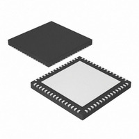
DSPIC33FJ64GS406-E/MR Microchip Technology, DSPIC33FJ64GS406-E/MR Datasheet - Page 251

DSPIC33FJ64GS406-E/MR
Manufacturer Part Number
DSPIC33FJ64GS406-E/MR
Description
MCU/DSP 16BIT 64KB FLASH 64QFN
Manufacturer
Microchip Technology
Series
dsPIC™ 33Fr
Datasheet
1.DSPIC33FJ32GS406-IPT.pdf
(418 pages)
Specifications of DSPIC33FJ64GS406-E/MR
Program Memory Type
FLASH
Program Memory Size
64KB (64K x 8)
Package / Case
64-VQFN
Core Processor
dsPIC
Core Size
16-Bit
Speed
40 MIPs
Connectivity
I²C, IrDA, LIN, SCI, SPI, UART/USART, USB
Peripherals
Brown-out Detect/Reset, QEI, POR, PWM, WDT
Number Of I /o
58
Ram Size
8K x 8
Voltage - Supply (vcc/vdd)
3 V ~ 3.6 V
Data Converters
A/D 16x10b
Oscillator Type
Internal
Operating Temperature
-40°C ~ 125°C
Product
DSCs
Data Bus Width
16 bit
Processor Series
DSPIC33F
Core
dsPIC
Numeric And Arithmetic Format
Fixed-Point or Floating-Point
Instruction Set Architecture
Harvard
Device Million Instructions Per Second
40 MIPs
Maximum Clock Frequency
120 MHz
Number Of Programmable I/os
58
Data Ram Size
4 KB
Operating Supply Voltage
3.3 V
Maximum Operating Temperature
+ 125 C
Mounting Style
SMD/SMT
3rd Party Development Tools
52713-733, 52714-737, 53276-922, EWDSPIC
Development Tools By Supplier
PG164130, DV164035, DV244005, DV164005, PG164120, DM240001, DV164033
Interface Type
I2C, SPI, UART
Minimum Operating Temperature
- 40 C
On-chip Adc
10 bit, 16 Channel
Lead Free Status / RoHS Status
Lead free / RoHS Compliant
Eeprom Size
-
Lead Free Status / Rohs Status
Lead free / RoHS Compliant
- Current page: 251 of 418
- Download datasheet (3Mb)
REGISTER 16-23: LEBCONx: LEADING-EDGE BLANKING CONTROL REGISTER
2010 Microchip Technology Inc.
bit 15
bit 7
Legend:
R = Readable bit
-n = Value at POR
bit 15
bit 14
bit 13
bit 12
bit 11
bit 10
bit 9-6
bit 5
bit 4
bit 3
bit 2
bit 1
bit 0
dsPIC33FJ32GS406/606/608/610 and dsPIC33FJ64GS406/606/608/610
Note 1: The blanking signal is selected via the BLANKSEL bits in the AUXCONx register.
R/W-0
PHR
U-0
—
PHR: PWMxH Rising Edge Trigger Enable bit
1 = Rising edge of PWMxH will trigger Leading-Edge Blanking counter
0 = Leading-Edge Blanking ignores rising edge of PWMxH
PHF: PWMxH Falling Edge Trigger Enable bit
1 = Falling edge of PWMxH will trigger Leading-Edge Blanking counter
0 = Leading-Edge Blanking ignores falling edge of PWMxH
PLR: PWMxL Rising Edge Trigger Enable bit
1 = Rising edge of PWMxL will trigger Leading-Edge Blanking counter
0 = Leading-Edge Blanking ignores rising edge of PWMxL
PLF: PWMxL Falling Edge Trigger Enable bit
1 = Falling edge of PWMxL will trigger Leading-Edge Blanking counter
0 = Leading-Edge Blanking ignores falling edge of PWMxL
FLTLEBEN: Fault Input Leading-Edge Blanking Enable bit
1 = Leading-Edge Blanking is applied to selected fault input
0 = Leading-Edge Blanking is not applied to selected fault input
CLLEBEN: Current-Limit Leading-Edge Blanking Enable bit
1 = Leading-Edge Blanking is applied to selected current-limit input
0 = Leading-Edge Blanking is not applied to selected current-limit input
Unimplemented: Read as ‘0’
BCH: Blanking in Selected-Blanking Signal High Enable bit
1 = State blanking (of current-limit and/or fault input signals) when selected blanking signal is high
0 = No blanking when selected blanking signal is high
BCL: Blanking in Selected-Blanking Signal Low Enable bit
1 = State blanking (of current-limit and/or fault input signals) when selected blanking signal is low
0 = No blanking when selected blanking signal is low
BPHH: Blanking in PWMxH High Enable bit
1 = State blanking (of current-limit and/or fault input signals) when PWMxH output is high
0 = No blanking when PWMxH output is high
BPHL: Blanking in PWMxH Low Enable bit
1 = State blanking (of current-limit and/or fault input signals) when PWMxH output is low
0 = No blanking when PWMxH output is low
BPLH: Blanking in PWMxL High Enable bit
1 = State blanking (of current-limit and/or fault input signals) when PWMxL output is high
0 = No blanking when PWMxL output is high
BPLL: Blanking in PWMxL Low Enable bit
1 = State blanking (of current-limit and/or fault input signals) when PWMxL output is low
0 = No blanking when PWMxL output is low
R/W-0
PHF
U-0
—
W = Writable bit
‘1’ = Bit is set
R/W-0
R/W-0
BCH
PLR
R/W-0
R/W-0
BCL
PLF
Preliminary
U = Unimplemented bit, read as ‘0’
‘0’ = Bit is cleared
FLTLEBEN
R/W-0
R/W-0
BPHH
(1)
CLLEBEN
(1)
R/W-0
R/W-0
BPHL
x = Bit is unknown
R/W-0
BPLH
U-0
—
DS70591C-page 251
R/W-0
BPLL
U-0
—
bit 8
bit 0
Related parts for DSPIC33FJ64GS406-E/MR
Image
Part Number
Description
Manufacturer
Datasheet
Request
R

Part Number:
Description:
IC, DSC, 16BIT, 12KB, 40MHZ, 3.6V, DIP28
Manufacturer:
Microchip Technology
Datasheet:

Part Number:
Description:
Manufacturer:
Microchip Technology Inc.
Datasheet:

Part Number:
Description:
Manufacturer:
Microchip Technology Inc.
Datasheet:

Part Number:
Description:
Manufacturer:
Microchip Technology Inc.
Datasheet:

Part Number:
Description:
Manufacturer:
Microchip Technology Inc.
Datasheet:

Part Number:
Description:
Manufacturer:
Microchip Technology Inc.
Datasheet:

Part Number:
Description:
Manufacturer:
Microchip Technology Inc.
Datasheet:

Part Number:
Description:
Manufacturer:
Microchip Technology Inc.
Datasheet:

Part Number:
Description:
Manufacturer:
Microchip Technology Inc.
Datasheet:


